CoWoS-L stays the packaging path through 2028 — the stuck step is still the package
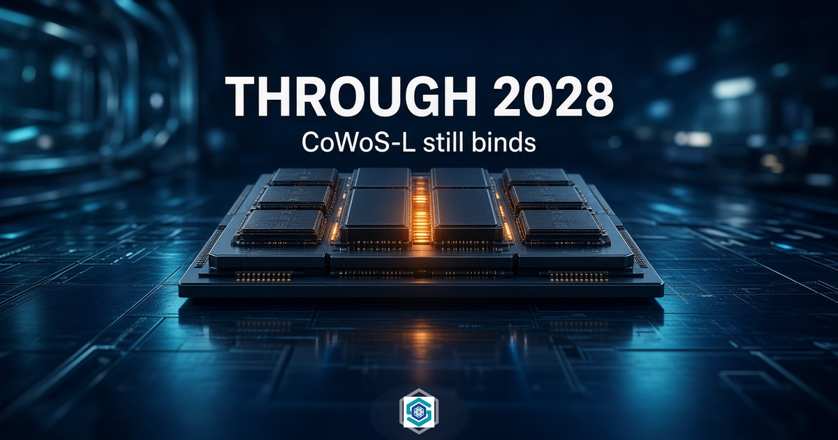
TrendForce keeps CoWoS-L as the mainstream AI packaging path through 2028. Packaging, not wafer starts, still sets the short clock.
WIRE · SEMICONDUCTORS · TAIWAN · Data as at 18 Sep 2026 · Updated 23 Sep 2026
TSMC's CoWoS-L stays the default package for large AI chips through 2028, TrendForce says, even as Intel's EMIB-T wins its first hyperscaler designs. For investors the stuck step is still the package, and the second-order money sits with the suppliers both packages need.
What happened
On 18 September 2026 TrendForce said TSMC's CoWoS-L is expected to remain the mainstream advanced-packaging platform for AI chips through 2028, ahead of Intel's EMIB-T on technology maturity and yield (TrendForce press centre, 18 Sep 2026).
The reason is size. As AI chips grow and carry more HBM stacks, the silicon interposer under them is reaching its physical limits. CoWoS-L gets around that by embedding small silicon bridge dies in the interposer, which allows packages several times the size of a single lithography field.
| Package | What it fits | Users TrendForce names |
|---|---|---|
| TSMC CoWoS-S | Two SoCs or chiplets plus eight HBM modules | Microsoft Maia 200 |
| TSMC CoWoS-L | More chiplets and more HBM | NVIDIA and AMD accelerators; Meta MTIA 400; AWS and Microsoft expected in 2027 |
| Intel EMIB-T | Bridges in the substrate, no large interposer | Google expected in 2027; AWS testing |
Why the package became the limit. A lithography machine prints one chip area at a time, a field of about 26 by 33 millimetres. The biggest AI processors already fill most of that field, and a single accelerator now sits beside several stacks of HBM memory that all have to be wired to it within millimetres. The interposer is the thin slab of silicon that carries those wires. Make it bigger and it gets harder to manufacture without defects, and it becomes a larger share of what the finished chip costs. CoWoS-L keeps the fine silicon wiring only where it is needed, in small embedded bridges, so the package can grow past one field without one giant, fragile slab of silicon.
Demand behind it, per the same release: NVIDIA's high-end GPU shipments are expected to grow about 30% in 2026; AMD is pushing its MI400/MI450 series from the second half of 2026; Google is expected to lead custom-chip volumes with TPU v7; and AWS is moving to Trainium v3 from the second half of 2026.
Why cash cares
On the semiconductors layer, the short clock is packaging: how much capacity exists, and which package architecture can actually ship. It is not only wafer starts. In our Taiwan CoWoS pulse, TrendForce put CoWoS demand about 20% ahead of supply in mid-2026, narrowing to about 10% by year-end, with reported capacity near 130,000 wafers a month by end-2026 and roughly double that by end-2028.
Who gets paid while packages grow is whoever can deliver CoWoS-L at volume with yield. CoWoS-L needs a larger interposer, so it costs more per chip. TrendForce says that cost, plus TSMC's tight capacity, is exactly why buyers are looking at EMIB. Designs that fit CoWoS-S wait less. Designs that need more chiplets and HBM stacks queue for CoWoS-L.
Since 18 September: the EMIB-T yield clock
On 23 September TrendForce reported, citing industry sources, that EMIB substrate yields have improved to about 45%, from about 30% in the second quarter. The supply chain is reportedly aiming for about 50% by the fourth quarter of 2026 and about 60% by the first quarter of 2027 (TrendForce, 23 Sep 2026 — reported).
The hard part moves into the substrate. EMIB-T embeds silicon bridges in the ABF substrate itself, and silicon and substrate expand at different rates under heat, so keeping each bridge seated and flush through repeated high-temperature steps is difficult. A new film under the bridges can also trap air during bonding, according to Common Wealth Magazine as cited by TrendForce.
Intel CEO Lip-Bu Tan said earlier this month that advanced packaging is Intel's next major growth area and that substrates are a bottleneck; Intel "has to prepay" suppliers, he said, naming four major partners, two in Japan and two in Taiwan. ZDNet, cited in the same report, lists Ibiden, Shinko Electric and Unimicron in the EMIB-T substrate chain, with Samsung Electro-Mechanics and LG Innotek trying to enter.
Our read: at about 45% yield, EMIB-T is a 2027 option, not a 2026 escape valve. That is why CoWoS-L stays the default.
The second-order read
| Who | Where they sit | What this means |
|---|---|---|
| TSMC | CoWoS-L capacity | Keeps pricing power on the largest AI packages through 2028 |
| HBM makers | More stacks per package | CoWoS-L exists to fit more HBM; each step to a bigger package raises memory content per accelerator |
| Substrate makers | Under both CoWoS and EMIB-T | EMIB-T moves hard integration into the substrate; Ibiden has reportedly secured upfront payments from Google, Amazon and Intel |
| Intel | EMIB-T | A 2027 customer foothold that depends on the yield path |
| Hyperscaler chip teams | Google, AWS, Microsoft | Two packaging routes lower dependence on one queue |
By market. In Taiwan, the read is TSMC's packaging mix and Unimicron's substrate position. In Korea, it is HBM content per package for SK hynix and Samsung, plus Samsung Electro-Mechanics' push into EMIB-T substrates. In Japan, it is Ibiden and Shinko Electric, the incumbents Intel is prepaying. In the US, it is Intel's packaging business finding outside customers, and the hyperscaler chip teams gaining a second route.
For the memory side, see HBM explained and the Korea HBM pulse. For the substrate side, see IC substrates and ABF explained.
Why 2027 is the crunch year
Line up the dates in TrendForce's release and the pressure lands in one year. AWS and Microsoft are expected to move custom chips onto CoWoS-L in 2027. Google is expected to start EMIB-T that same year, and AWS is testing it. The EMIB substrate yield target of about 60% falls in the first quarter of 2027. So 2027 is when CoWoS-L demand widens from GPU makers to hyperscaler chip teams, while the only alternative is still climbing its yield curve.
Our read: whoever holds CoWoS-L capacity in 2027 holds the schedule for most of the large AI chips that ship that year. The chips that ship on time are the ones whose packaging slot is booked, not the ones with the best design. That is why the package, not the wafer, is still the stuck step to watch.
Two cautions
These are forecasts and reports, not orders. TrendForce's through-2028 view is a research call, and the EMIB yield figures come from unnamed industry sources, not from Intel. The capacity numbers in our Taiwan pulse are reported targets, not disclosed output. And adoption dates for custom chips move often; a single programme slipping a year changes which package it needs.
What would change the view
- EMIB substrate yields reaching about 60% by the first quarter of 2027 on schedule, with Google confirming EMIB-T volume that year: spillover out of TSMC's queue arriving sooner.
- TSMC's CoWoS capacity catching up with demand before end-2026, closing the ~10% gap TrendForce expects.
- AWS or Microsoft keeping 2027 custom chips on CoWoS-S, or moving them to EMIB-T, instead of CoWoS-L.
What to watch
- Q4 2026: whether EMIB substrate yields reach about 50%.
- TSMC Q3 2026 results (October): comments on advanced-packaging capacity and CoWoS-L mix.
- 2027 custom-chip programmes: AWS and Microsoft packaging confirmations.
- Second half of 2026: AMD MI400/MI450 volume, which adds to CoWoS-L demand.
Read: TSMC, CoWoS Capacity and the Packaging Gate and Foundry and Advanced Packaging Explained for how packaging sits on the map.
Get the Wire. A free brief every day, here and in your inbox. Subscribe free →
Sources: TrendForce, 18 Sep 2026 — company press; TrendForce, 23 Sep 2026 — reported, citing industry sources, Common Wealth Magazine and ZDNet. Not investment advice.