
What Is a Clean Room? Why Chip Supply Waits on Empty Space
A clean room is a sealed room where air is filtered so few particles land on a wafer. New chip supply waits on these rooms: Samsung says it secures clean rooms first and adds tools later, so 2027 capex buys little 2028 output.

EXPLAINED · Mechanism · Last reviewed: 30 Oct 2026 · Next review: after Samsung’s P5 tool move-in (reported for mid-2027) or SEMI’s next 300mm Fab Outlook
A clean room is a sealed room where the air is filtered and kept moving so that almost no dust lands on the silicon wafers chips are made from.
In short. A clean room is the filtered-air space inside a chip fab where wafers are processed. It has to be built before a single production tool can be installed, and it takes the longest to add. That is why Samsung said on 29 October 2026 that much of next year’s higher capex will buy new space, not new chips, and that 2027 spending is unlikely to lift 2028 output much. Our read: the builders of clean rooms are paid first, the tool makers next, and the chipmaker last; the stuck step is the room itself.
Why an investor cares: a chipmaker can have the cash and the orders and still not ship more chips, because new output waits on new clean rooms. Samsung made a record ₩107.4 trillion of operating profit in July–September 2026 and still said supply stays tight into 2028; our Korea note on Samsung’s third quarter covers the numbers. This page covers the room that sets the pace.
What is a clean room?
A clean room is the part of a chip factory, or fab, where wafers are actually processed. Air is pushed down from filters that cover the ceiling, passes over the work and leaves through holes in a raised floor, so particles are swept away before they settle.
Dust is only part of the job. A semiconductor clean room also holds temperature and humidity in a narrow band and controls static electricity, stray electromagnetic fields and vibration. Small changes in any of these can spoil a pattern on a wafer.
Under the floor and above the ceiling sit the utilities: ultra-pure water, process gases, chemical lines, exhaust and power. In a large fab these support systems fill whole floors above and below the clean room.
Why do chips need a clean room?
Because the features on a modern chip are far smaller than a speck of dust. A single particle that lands at the wrong step can bridge two wires or block a pattern, and the chip under it fails.
Every failed chip is output the fab paid to make and cannot sell. So cleanliness feeds straight into yield, the share of chips on a wafer that work. Our guide to EUV lithography covers the step where patterns are smallest and the air matters most.
Modern fabs add a second layer. Wafers travel between tools inside sealed plastic pods, and each tool has its own filtered mini-environment, so the air touching the wafer is cleaner than the room around the workers.
What are clean room classes?
Clean rooms are graded under ISO 14644-1, an international standard last revised in 2015. A room’s class is set by the most particles of a given size allowed in each cubic metre of air, counted with laser particle counters.
Each class up allows about ten times more particles. An ISO Class 5 room allows at most 3,520 particles of 0.5 micrometres or larger per cubic metre. Class 9, roughly the air in an ordinary office, allows 35.2 million, about 10,000 times more.
| ISO 14644-1 class | Max particles ≥0.1 µm per m³ | Max particles ≥0.5 µm per m³ | Where you meet it (our read) |
|---|---|---|---|
| Class 1 | 10 | not set | The cleanest classified air; small sealed zones |
| Class 3 | 1,000 | 35 | Air around wafers in advanced chip lines |
| Class 5 | 100,000 | 3,520 | Many chip process bays; also sterile drug filling |
| Class 7 | not set | 352,000 | Assembly, some electronics and medical device rooms |
| Class 9 | not set | 35,200,000 | Roughly ordinary indoor air |
Limits from the ISO 14644-1:2015 class formula. The right-hand column is Second Order’s read of typical use, not part of the standard.
The older US Federal Standard 209E used names such as “Class 100” for particles per cubic foot. ISO 14644-1 replaced it, but the old names still appear in trade press; Class 100 is roughly ISO Class 5.
How long does a clean room take to build?
Most of a year before tools move in, and 18 months to two years before new output. The clean room is the first big piece of a fab to be built and the last thing that can be rushed.
Samsung’s P5 site at Pyeongtaek in South Korea shows the order. ZDNet Korea reported on 28 September 2026 that the clean room for P5’s first line began in the third quarter of 2026, about six months earlier than planned. Tool move-in is being discussed for May–June 2027, and P5 targets operation in 2028.
| Step | Example, as reported | What it tells you |
|---|---|---|
| Clean room build starts | Samsung P5 phase 1, Pyeongtaek: third quarter of 2026, about six months earlier than first planned | The shell is the first big spend |
| Tools move in | P5 phase 1: discussed for May–June 2027, pulled forward from July–August 2027 | Roughly 8 to 11 months after the room starts |
| Output | P5: operation targeted for 2028 | New bits arrive 18 months to two years after the room starts |
| Room running, tools going in | Samsung Taylor Fab 1, Texas: clean room operating, tools being installed, line-setup wafers running (29 Oct 2026) | A finished room still is not output |
| Builder’s revenue | L&K chip projects booked over about 18–24 months; most of UIS’s backlog over 24–36 months | The contractor is paid through the build, years before the chips |
From Samsung’s 29 October 2026 call, ZDNet Korea (28 September 2026) and Commercial Times (5 October 2026). The middle-column timings for P5 are reported, not Samsung guidance. Right-hand column: Second Order’s read.
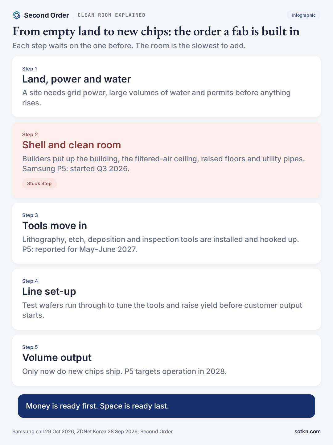
A finished room is still not output. On 29 October Samsung said its Taylor, Texas Fab 1 has started clean room operations and tool installation, with wafers running only to set up the line. Our Wire on Samsung’s Taylor fab covers who it is being built for.
Why does chip supply wait on clean rooms?
Because space is the slowest input to add. Tools can be ordered, stored and moved, but a clean room has to be designed, built and certified on site, and there is only so much of it standing empty at any time.
Samsung said this plainly on 29 October. It expects industry capex to rise significantly in 2027, but said much of the increase will go on acquiring new space, higher construction costs make the numbers look bigger, and the long lead time from new fab construction to wafer output means 2027 spending is unlikely to lift 2028 output much.
Its answer is to build ahead: secure clean rooms in advance, then add tools flexibly as demand moves. Our read: that turns empty space into an option the company can fill quickly, at the cost of paying for buildings before they earn. Our Analysis on what happens if new clean rooms sit empty in 2028 works through the downside of that option.
How much is being spent on clean rooms?
More each year to 2028. SEMI, the chip equipment industry body, projected on 13 October 2026 that construction spending on 300mm fabs will rise 23% to $47.5 billion in 2026, 33% to $63.3 billion in 2027 and to $68.4 billion in 2028.
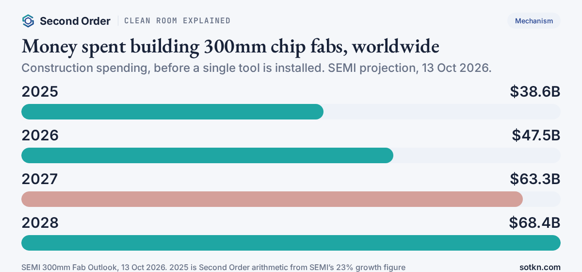
Our arithmetic: that puts 2025 at about $38.6 billion, so construction spending rises about 77% in three years. SEMI expects 20 new 300mm fabs or lines to start construction in 2026 and 18 in 2027, and 13 to begin operating in 2026 rising to 23 in 2027.
Equipment is still the larger bill. SEMI put 300mm equipment spending at $149 billion for 2026, so on our arithmetic about $1 goes on buildings for every $3 on tools. The tools only go in once the room is ready; our guide to who makes wafer fab equipment covers that side of the bill.
Who gets paid, and where is the stuck step?
The clean room builders are paid first. Specialist facility contractors design and build the room, the air system, the raised floors and the utility pipes, and book revenue as the work progresses, long before the chipmaker sells anything from it.
Taiwan’s contractors show the scale. Taiwan News reported on 15 September 2026 that L&K Engineering’s revenue for January–August rose 63.4% to NT$67.9 billion and United Integrated Services (UIS) rose 71.6% to NT$65.7 billion, both records. Yankey Engineering more than doubled to NT$28.2 billion.
Their order books run years ahead. L&K reported NT$440.1 billion, about US$13.9 billion, of signed work not yet booked, and UIS NT$193.9 billion, about US$6.1 billion. Our arithmetic: at this year’s pace that is about 4.3 years of revenue for L&K and about 2.0 years for UIS.
Singapore is part of the pipeline. Commercial Times reported on 5 October that L&K treats Taiwan and Singapore as its two growth engines, and on 27 July that it won the facility contract for Micron’s new Singapore fab, alongside projects by VSMC and UMC there. Our Singapore Markets door tracks the data centre side of the same island.
Tool makers are paid next, when equipment moves into the finished room. That is the moment the bill shifts to companies such as ASML, Applied Materials, Lam Research, Tokyo Electron and KLA.
The chipmaker is paid last, when wafers come out and chips ship, 18 months to two years after the room was started. Our read: the stuck step is the clean room itself. Its builders are short of people, not orders: contractors said at investor briefings, as Commercial Times reported in July, that the challenge is finishing on time amid supply-chain issues, labour shortages and too few engineering managers.
What would change the view?
- Rooms finish faster. If Samsung’s P5 tools move in on the earlier May–June 2027 date and output starts early in 2028, the clock from room to chips shortens.
- Demand cools before the rooms fill. Samsung’s build-ahead plan means paying for space first. If demand slips, rooms sit empty and the tool orders are the part that gets cut.
- Contractors stop finding people. If labour and engineering managers stay short, backlog stretches beyond the 18–36 months the builders expect, and every fab behind them slips with it.
What to check next
Watch Samsung’s P5 tool move-in date, SEMI’s next 300mm Fab Outlook and the Taiwan contractors’ monthly sales, which come out around the 10th of each month. Our Analysis on Micron’s clean room stuck step covers the same clock at another memory maker, and our guide to HBM covers the memory most of the new space is for.
Common misconceptions
- People assume more capex means more chips next year. Actually Samsung said much of the 2027 capex rise buys new space, and the lead time from construction to wafers means little extra 2028 output.
- People assume a clean room is just a very clean room. Actually it is a full machine: ceiling filters, raised floors, ultra-pure water, gases, exhaust, and control of temperature, humidity, static and vibration.
- People assume a finished clean room means output. Actually tools still have to move in and the line has to be set up with test wafers; Samsung’s Taylor Fab 1 is at that stage now.
- People assume the chipmaker is paid first in a fab boom. Actually the contractors who build the rooms book revenue through the build, years before the new chips ship.
FAQ
What is a clean room?
A clean room is a sealed room where the air is filtered and kept moving so that almost no dust lands on the silicon wafers chips are made from. It also holds temperature, humidity, static and vibration steady.
Why do semiconductors need a clean room?
Because the features on a modern chip are far smaller than a speck of dust. One particle landing on a wafer at the wrong step can short or break a circuit, and every ruined chip is output the fab paid for and cannot sell.
What are clean room classes?
Clean rooms are graded under the ISO 14644-1 standard by how many particles are allowed in each cubic metre of air. An ISO Class 5 room allows at most 3,520 particles of 0.5 micrometres or larger per cubic metre; Class 9, roughly ordinary room air, allows 35.2 million.
How long does it take to build a semiconductor clean room?
Most of a year before tools move in, and 18 months to two years before output. Samsung began the first clean room at its P5 site in Pyeongtaek in the third quarter of 2026; tools are reported to move in around May–June 2027, with operation targeted for 2028.
Why does Samsung build clean rooms first?
Because space is the slowest part to add. Samsung said on 29 October 2026 that it secures clean rooms in advance and then adds equipment flexibly as demand moves, since tools can be ordered later but a room cannot be built quickly.
Who builds semiconductor clean rooms?
Specialist facility contractors. In Taiwan they include L&K Engineering, United Integrated Services, Marketech and Yankey Engineering, whose revenue and order books hit records in 2026 on chip fab projects in Taiwan, the US and Singapore.
Is this a list of stocks to buy or sell?
No. This page explains what a clean room is and why it sets the pace of new chip supply. It does not rank companies or give buy or sell calls. Not investment advice. Do your own research.
Related: who makes wafer fab equipment; EUV lithography; HBM; memory process tools; cash capex; how long an AI data centre takes to build.
Stack doors
Layer: Semiconductors. Also: SK hynix, Micron and TSMC. Markets: Korea, Taiwan.
Get the Wire — short daily notes when fab builds and chip supply move.
Not investment advice. Do your own research.
How we check this
Samsung’s statements on clean rooms, capex and its Taylor fab come from its 29 October 2026 earnings call. The P5 timings are as reported by ZDNet Korea on 28 September 2026 and are not company guidance. Fab construction spending comes from SEMI’s 13 October 2026 outlook. Clean room classes come from the ISO 14644-1:2015 standard. Contractor revenue, order books and booking periods come from Taiwan News (15 September 2026) and Commercial Times (27 July and 5 October 2026), which report the companies’ own monthly sales and investor briefings. The 2025 construction figure, the years-of-backlog figures, the US dollar conversions and the construction-to-equipment ratio are our arithmetic and are labelled as ours on the page. The order of who gets paid, the typical-use column and the stuck step are our read. The featured photograph is credited in its caption. This page explains what a clean room is. It does not rank companies or give buy or sell calls. Not investment advice. Do your own research.
Last reviewed: 30 Oct 2026 · Next review: after Samsung’s P5 tool move-in (reported for mid-2027) or SEMI’s next 300mm Fab Outlook
Spot an error? Tell us and we will correct it and note the change here.
References
- Samsung Electronics — Q3 2026 earnings call transcript, via Stock Analysis (Quartr) (29 Oct 2026) — much of the 2027 capex rise buys new space; long lead time from fab construction to wafer output; clean rooms secured in advance, tools added flexibly; Taylor Fab 1 clean room operations, tool installation and line-setup wafers; 2026 capex ₩84.4 trillion, ₩29 trillion in Q3
- ZDNet Korea — Samsung speeds up first P5 production line; tool move-in pulled to Q2 2027 (Korean) (28 Sep 2026) — P5 phase 1 clean room build started in Q3 2026, about six months early; tool move-in discussed for May–June 2027 instead of July–August; P5 targets operation in 2028; long equipment lead times
- SEMI — Global 300mm fab equipment spending to reach $227 billion in 2029, 300mm Fab Outlook (13 Oct 2026) — 300mm fab construction spending $47.5B in 2026 (+23%), $63.3B in 2027 (+33%), $68.4B in 2028; equipment spending $149B in 2026; 20 fabs or lines start construction in 2026 and 18 in 2027; 13 begin operating in 2026 and 23 in 2027
- ISO — ISO 14644-1:2015, Cleanrooms and associated controlled environments, Part 1: classification of air cleanliness by particle concentration (Dec 2015; confirmed 2021) — the class system, counted for particles from 0.1 to 5 micrometres with light-scattering particle counters
- Taiwan News — Taiwan cleanroom engineering firms hit record revenue on chip investment (15 Sep 2026) — L&K Engineering revenue NT$67.9B in January–August (+63.4%), backlog NT$440.1B over about three years; UIS revenue NT$65.7B (+71.6%), backlog NT$193.9B; Yankey NT$28.2B (+112.8%); what a clean room controls
- Commercial Times (工商時報) — Fab-building demand keeps L&K and UIS order books full (Chinese) (5 Oct 2026) — chip projects recognised over about 18 to 24 months at L&K and most of UIS’s backlog over 24 to 36 months; fab plans extend to 2029; Taiwan and Singapore as L&K’s two growth engines
- Commercial Times (工商時報) — Facility engineering orders strong, on-time delivery is the challenge (Chinese) (27 Jul 2026) — contractors say the challenge is finishing on time amid supply-chain issues, labour shortages and too few engineering managers; Singapore fab projects including VSMC, UMC Fab 12i and a planned Micron NAND complex; L&K’s Micron Singapore turnkey contract