What Is EUV? Extreme Ultraviolet Lithography for AI Dies
EUV lithography prints the tightest layers on a leading-edge die. Who gets paid when Low-NA scanners are booked, and why High-NA is a later clock.
EXPLAINED · Mechanism · Last reviewed: 30 Sep 2026 · Next review: after ASML Q3 2026 results print Low-NA EUV shipments against the ~65 plan
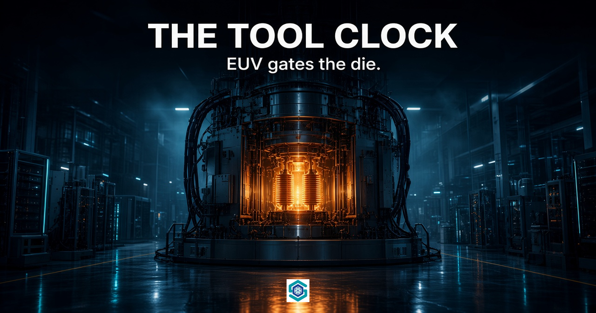
EUV lithography is the scanner step that prints the tightest layers on a leading-edge die: a machine shines 13.5-nanometre light through a mask onto a photoresist-coated wafer so the foundry can cut features that older ultraviolet light cannot print in one exposure.
In short. EUV is how the semiconductors layer turns a mask into a transistor pattern. The stuck step on the tool clock is Low-NA output — about 65 systems this year, already close to fully ordered for 2027 — not a High-NA headline. A die that never gets those layers does not reach CoWoS. A packaged module still waits on HBM. Those are neighbour clocks, not the same one.
Who gets paid when AI accelerators need more EUV layers per wafer, and which clock you are watching — the Low-NA box, the High-NA insertion, or the packaging slot after the die is printed.
What is EUV lithography?
Lithography is how a foundry draws the circuit. Light hits a mask, the mask throws a shadow onto resist, and the pattern becomes the transistor. Deep ultraviolet (DUV) uses longer-wavelength light. Extreme ultraviolet (EUV) uses 13.5-nanometre light so a single exposure can print tighter pitches instead of stacking several DUV passes.
The machine is a scanner. ASML is the only company that sells production EUV scanners. Low-NA systems (the NXE family, numerical aperture 0.33) are the volume workhorses. High-NA systems (the EXE family, numerical aperture 0.55) print a smaller field at higher resolution. They are not interchangeable boxes on the same clock.
| Shape | What it prints | 2026 volume print | If the foundry waits |
|---|---|---|---|
| DUV immersion | Wider pitches; multi-patterning on older nodes | ~130 immersion shipments planned (ASML Q2 2026) | Mainstream and memory layers still move |
| Low-NA EUV | Tight layers on 7 nm-class and below, including N3/N2 and advanced DRAM | ~65 systems planned; already most of the EUV invoice | Leading-edge dies queue |
| High-NA EUV | Tighter layers, smaller exposure field | One system recognised in Q2 2026 revenue | A later insertion clock, not this year's 65 |
ASML's Q2 2026 call is the dated seller print. Net system sales were €6.6 billion, of which €3.8 billion was EUV systems — including one High-NA — and €2.8 billion was non-EUV. Logic was 51% of net system sales, memory 49% (investor call, 15 Jul 2026). Our check: 3.8 ÷ 6.6 = 58% of the system invoice was EUV. 3.8 ÷ 9.326 = 41% of total net sales (€9.326 billion in the 6-K). The rest of the quarter was DUV, metrology, and Installed Base Management (€2.762 billion of service and field options).
EUV is a tool. Foundry and advanced packaging is the finish line after the die exists. Memory process tools are the equipment gate behind HBM stacks. EUV sits earlier: no printed leading-edge die, nothing for CoWoS to join.
Why does EUV bind?
It binds because there is one qualified maker, a finite number of boxes this year, and more EUV layers per wafer as nodes shrink. A foundry can announce a capital budget. It cannot print N2 layers without a scanner that has been built, installed, and qualified.
ASML's 15 Jul 2026 6-K is the capacity clock: it plans to add 30% to 2026 Low-NA EUV capacity of around 65 for 2027, and is investigating another 30% for 2028. The same step applies to DUV immersion from a 2026 base of around 130. Our arithmetic: 65 × 1.30 = 84.5, the ~85 Low-NA boxes the call treated as 2027's balance of demand and supply. 65 × 1.30 × 1.30 = 109.85, the ~110 case it said it was investigating for 2028 — investigating, not a booked shipment plan. CFO Roger Dassen said 2027 Low-NA is "close to being fully covered with orders" (investor call, 15 Jul 2026). A 30% add that is already spoken for is not an open queue.
The buyer print sits in Taiwan. TSMC's Q2 2026 release said 2-nanometer was 3% of wafer revenue, 3 nm 30%, 5 nm 33%, 7 nm 11%. Advanced nodes (7 nm and below) were 77% of wafer revenue. HPC was 66% of net revenue (16 Jul 2026). Those are the nodes that consume EUV. Inventory days rose to 87 "primarily due to the ramp of N2 technology" (Q2 2026 call). CFO Wendell Huang said the 2026 capital budget was raised to US$60 billion to US$64 billion, with about 70% to 80% for advanced process technologies and 10% to 20% for advanced packaging, testing, mask making and others. Our check on the midpoint: 70% of 62 is about US$43 billion aimed at process tools — the bucket EUV sits in — versus US$6–12 billion in the packaging/test/mask band. A larger foundry cheque does not mint 65+1 scanners this year. It orders them into ASML's already-covered years.
High-NA is a different clock. ASML said on 15 Jul 2026 that Intel Foundry is using High-NA on Intel 18A for a subset of Core Ultra Series 3 (Panther Lake) layers, dual-qualified against the NXE (Low-NA) platform. Intel's 7 Sep 2026 SPIE update said more than one million wafers had been processed across tool certification, R&D, and volume production on select layers — not one million commercial Panther Lake wafers on High-NA alone. Overlay, throughput and availability "are meeting Intel Foundry's expectations." That is insertion evidence. It is not proof that High-NA has replaced the Low-NA 65.
China is the other bind. Dassen said China-related business should stay around 20% of total net sales for 2026, "mainly related to an increased demand in mainstream logic" (investor call). Mainstream logic is DUV territory. EUV remains a licensed, restricted tool. A domestic AI stack can buy hours and halls and still wait on a die that was never printed on an NXE.
Who gets paid — and where is the stuck step?
On the semiconductors layer, who gets paid tracks which lithography step has cleared.
| Step | Who | Why it matters |
|---|---|---|
| Tool | ASML (optics with Zeiss) | Only qualified EUV scanner seller; 58% of Q2 system sales was EUV |
| Stuck step | Low-NA output and install | ~65 boxes this year; 2027 already close to fully ordered |
| Foundry | TSMC, Samsung, Intel Foundry | Get paid when EUV layers yield and wafers ship |
| Neighbour gate | CoWoS-class packaging + HBM | A printed die still needs a stack and a slot |
| Buyer | Hyperscalers and accelerator designers | Pay for modules, not for scanner backlog |
Cash sticks at ASML when a Low-NA system is recognised (€3.8 billion of Q2 system sales) and when the installed base is upgraded (€2.762 billion of service and field options). Cash sticks at the foundry when N2 and N3 wafers leave — TSMC's 3% N2 mix in Q2 is the start of that invoice, with a "steep ramp" guided for Q3 (Wendell Huang, 16 Jul 2026). Cash sticks at packaging when Chairman C.C. Wei says capacity is "so tight that now it limits my customers' growth" (same call). Cash sticks in Korea when DRAM adds EUV layers: ASML guided memory-related net system sales to grow over 75% in 2026 as customers replace multi-patterning with single-expose Low-NA (Christophe Fouquet, 15 Jul 2026).
The US door is High-NA insertion — Intel's Oregon EXE line — not a neocloud hour. The Taiwan door is TSMC's process-tool share of the US$60–64 billion budget. Korea is DRAM lithography intensity beside HBM allocation. China is the 20% mainstream-logic slice that does not include EUV.
A useful test, not a ticker call: if ASML's Q3 and Q4 prints show Low-NA shipments tracking the ~65 plan while TSMC's N2 mix rises from 3%, the tool clock is converting. If Low-NA slips, or 2027 coverage stays full while foundries raise capex again, the scanner — not the slide — is still the bind. If High-NA revenue stays "one system a quarter" while Low-NA is sold out, do not read the Intel subset as this year's volume clock.
Common misconceptions
- People assume a foundry capex raise means more EUV this year. Actually TSMC's US$60–64 billion 2026 budget is a multi-year tool order. ASML's 2026 Low-NA plan is still about 65, and 2027 is already close to fully covered.
- People assume High-NA has taken over from Low-NA. Actually Q2 2026 recognised one High-NA system inside €3.8 billion of EUV sales. Intel's High-NA use is select 18A layers, dual-qualified to NXE. Fouquet said High-NA still has to reach Low-NA maturity before it beats Low-NA-plus-immersion on cost (15 Jul 2026).
- People assume EUV and CoWoS are the same bottleneck. Actually EUV prints the die. CoWoS joins the die to HBM. Wei's packaging bind can throttle modules even when front-end tools are installing. See CoWoS explained.
- People assume China 20% of ASML sales means China is buying EUV. Actually Dassen tied that 20% to mainstream logic. That is DUV. Export licensing is why the EUV box is a different door — China HBM access is the sibling stuck step on memory.
- People assume more DUV immersion (130 systems) substitutes for EUV on N2. Actually 2 nm is an EUV-intensity node. DUV still prints many layers. It does not replace the Low-NA exposures that make N2 a 3% wafer-revenue line.
Not investment advice. Do your own research.
FAQ
What is EUV lithography?
EUV lithography is the scanner step that prints the tightest layers on a leading-edge die using 13.5-nanometre light. ASML is the only company that sells production EUV scanners. Low-NA systems do today's volume; High-NA is a later insertion clock.
How is EUV different from DUV?
DUV uses longer-wavelength light and often needs several exposures to print a tight pitch. EUV uses 13.5-nanometre light so one exposure can print tighter layers. ASML still plans about 130 DUV immersion shipments in 2026 beside about 65 Low-NA EUV systems.
Why does EUV bind AI chip supply?
Because leading-edge AI dies need more EUV layers per wafer, there is one qualified scanner maker, and 2026 Low-NA output is about 65 systems with 2027 already close to fully ordered. A die that is not printed cannot be packaged.
Is High-NA EUV the same clock as Low-NA?
No. Low-NA is this year's volume clock. High-NA is insertion: ASML recognised one High-NA system in Q2 2026, and Intel is using it on select 18A layers that are also qualified on Low-NA tools.
Who gets paid when EUV scanners are scarce?
ASML gets paid when a scanner is recognised and when the installed base is upgraded. Foundries get paid when EUV layers yield. Packaging and HBM still get paid after the die exists. The stuck step is Low-NA output and install, not the High-NA press release.
Does more TSMC capex mean more EUV tools this year?
No. TSMC raised its 2026 capital budget to US$60–64 billion, with 70–80% for advanced process. That is a multi-year order book. ASML's 2026 Low-NA plan remains about 65 systems.
Can China buy EUV scanners?
Not as a mainstream path. ASML guided China-related sales at about 20% of 2026 total, mainly mainstream logic — DUV, not EUV. Export licensing is why the scanner and the domestic stack are different doors.
Related terms
- CoWoS — packaging twin that joins a printed die to HBM; a neighbour clock, not EUV.
- HBM — stacked memory the EUV-printed GPU still needs beside it.
- Foundry and advanced packaging — the wider finish line after lithography.
- Memory process tools — equipment gate behind HBM, parallel to EUV on the DRAM side.
- Who makes AI chips — the designer names that wait on printed, packaged modules.
Markets and stack doors
Layer: semiconductors. Sibling layers: hyperscalers (who buy the modules) · neoclouds (who bill the hours after the module ships). Markets: TSMC capex split · TSMC revenue · Korea chip exports · China HBM access.
Get the Wire — short notes when scanner or node clocks move. Stack: What Does TSMC Do? · What Does SK hynix Do?. Analysis: where the stuck step moves.
How we check this
Figures come from company filings and company releases, each dated in the list below. Capacity and timing from press reports are labelled as reported, not guided. Where we work something out ourselves, the arithmetic is shown in full.
Last reviewed: 30 Sep 2026 · Next review: after ASML Q3 2026 results print Low-NA EUV shipments against the ~65 plan
Spot an error? Tell us and we will correct it and note the change here.
Sources
- ASML Form 6-K — Q2 2026 total net sales €9.326B; 86 new lithography systems; Installed Base Management €2.762B; 2026 Low-NA EUV capacity around 65 with +30% planned for 2027; DUV immersion around 130; FY 2026 net sales €43–45B (15 Jul 2026)
- ASML Q2 2026 investor call transcript — net system sales €6.6B of which €3.8B EUV (including one High-NA) and €2.8B non-EUV; logic 51% / memory 49%; ~65 Low-NA shipments and >45% EUV system-sales growth; 2027 Low-NA close to fully covered; China ~20% of sales, mainly mainstream logic (15 Jul 2026)
- ASML High-NA EUV readiness — Intel Foundry using High-NA on select Intel 18A layers for a subset of Core Ultra Series 3, dual-qualified to the NXE platform (15 Jul 2026)
- Intel Foundry newsroom — more than one million wafers processed with High-NA across certification, R&D, and volume production on select Panther Lake layers (7 Sep 2026)
- TSMC Form 6-K — Q2 2026: 2 nm 3% of wafer revenue; 3 nm 30%; 5 nm 33%; 7 nm 11%; advanced (7 nm and below) 77% (16 Jul 2026)
- TSMC Q2 2026 earnings call — 2026 capital budget US$60–64B (70–80% advanced process, 10–20% packaging/test/mask); Q2 CapEx US$15.7B; N2 inventory-days 87; C.C. Wei: packaging capacity “so tight that now it limits my customers’ growth” (16 Jul 2026)