Who Makes AI Chips
Who makes AI chips is the map of roles along the stack — designers, foundries, packaging attach, and HBM. Roles only. No tip sheet.
EXPLAINED · Players · Last reviewed: 25 Sep 2026 · Next review: after next major foundry/packaging/HBM capacity note
Who makes AI chips is the roles map for AI accelerators: which firms design the GPU or ASIC, which foundries fabricate the logic wafers, which partners attach logic beside HBM on advanced packaging, and which memory makers supply the stacks.
In short. Who makes AI chips is a roles map on the semiconductors layer: accelerator designers own the GPU or ASIC; foundries fabricate logic wafers; advanced packaging attaches logic beside HBM; memory makers supply the stacks. The stuck step sits at scarce foundry, packaging, and HBM when CapEx orders bind — not a tip sheet.
For investors on the Semiconductors layer, the useful question is which role gets paid when AI CapEx binds scarce wafers, packaging, and HBM — not which ticker “wins.” For the memory roles map, see who makes HBM; for the attach gate, see what CoWoS is.
Who makes AI chips?
Who makes AI chips splits into four roles. Accelerator designers own the GPU or ASIC architecture. Foundries fabricate the logic wafers on advanced nodes. Advanced-packaging partners attach those dies beside HBM. Memory makers build the HBM cubes. Missing any one role leaves the rack waiting — even when CapEx is approved.
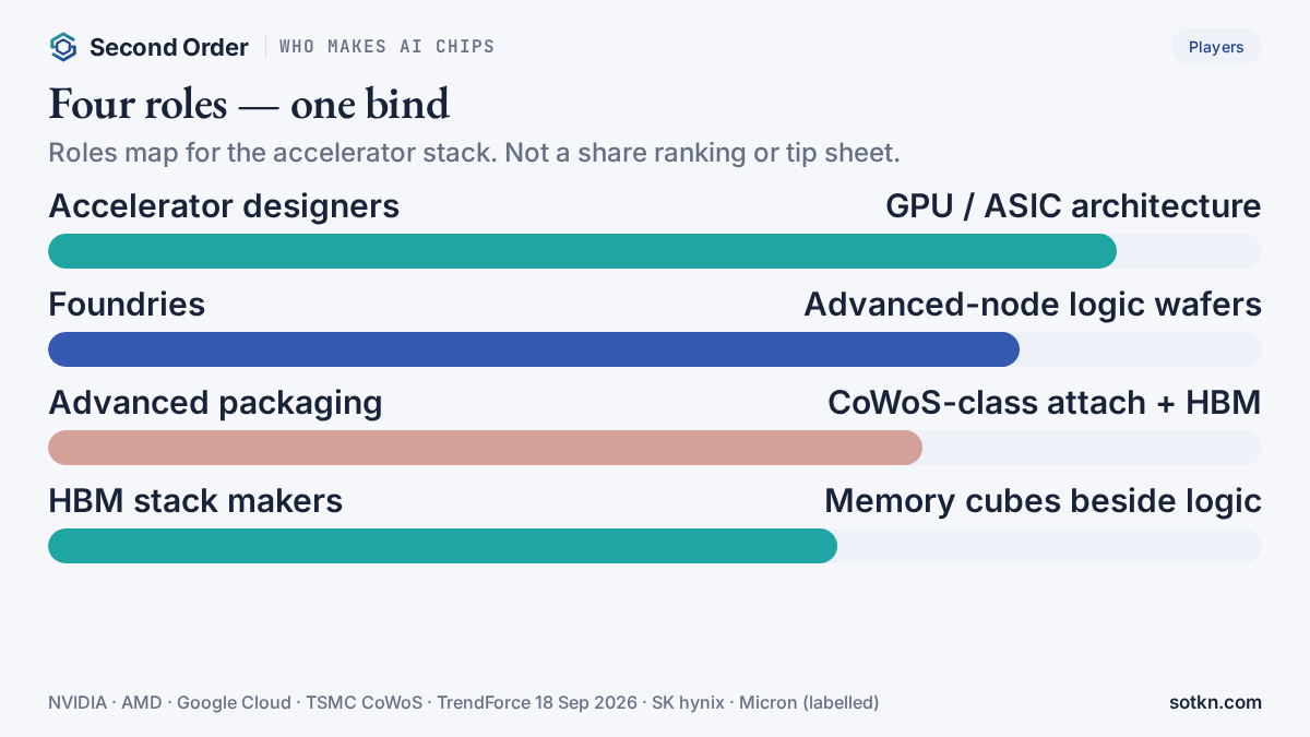
| Role | Job | Dated example (labelled) |
|---|---|---|
| Accelerator designers | Design the GPU / ASIC architecture and software stack | NVIDIA Blackwell platform (18 Mar 2024); Blackwell Ultra GB300 NVL72 (18 Mar 2025); AMD Instinct MI350 Series (12 Jun 2025); Google Trillium TPU GA (11 Dec 2024) |
| Foundries | Fabricate advanced-node logic wafers | TSMC advanced nodes for leading AI GPUs/ASICs; CoWoS packaging path documented on TSMC CoWoS page (accessed 25 Sep 2026) |
| Advanced packaging / attach | Place logic beside HBM on CoWoS-class package | TSMC CoWoS integrates SoC + HBM; CoWoS-L in volume since 2024. TrendForce: CoWoS-L mainstream through 2028 (18 Sep 2026, reported) |
| HBM / memory stack makers | Build DRAM cubes attached beside the accelerator | SK hynix 12-Hi HBM3E volume production (26 Sep 2024); Micron HBM3E 12-Hi >1.2 TB/s (5 Sep 2024) |
Who designs the accelerator?
Accelerator designers set the architecture and software stack. NVIDIA announced the Blackwell platform — including the GB200 Grace Blackwell Superchip and GB200 NVL72 rack-scale system — on 18 March 2024 (NVIDIA Newsroom). On 18 March 2025 it announced Blackwell Ultra with the GB300 NVL72 and HGX B300 (NVIDIA Newsroom) — company-reported product claims.
AMD unveiled the Instinct MI350 Series (MI350X / MI355X) on 12 June 2025 at Advancing AI (AMD IR). Hyperscaler custom ASICs sit in the same designer role: Google’s Trillium sixth-generation TPU reached general availability on 11 December 2024 (Google Cloud Blog). Those dates show the role, not a ranking — generations move; the job stays design.
Who fabricates the logic wafers?
Foundries turn the design into silicon. Leading AI GPUs and many custom ASICs run on TSMC advanced nodes, then move into advanced packaging. That is a foundry role — wafer fabrication — separate from designing the accelerator or building the DRAM stack. See foundry and advanced packaging.
When CapEx orders bind scarce advanced-node capacity, cash sticks at the foundry step even if designs are ready. Samsung Foundry also fabricates advanced logic for some customers — labelled by product, not as a share ranking.
Who attaches logic to HBM?
An AI accelerator only becomes useful when logic sits beside HBM on an advanced package. TSMC’s CoWoS family places SoCs and HBM stacks on an interposer or local-silicon-bridge package; CoWoS-L has been in volume production since 2024 (TSMC CoWoS page). That is packaging attach — not DRAM fabrication and not GPU design. For the memory side of the same bind, see what HBM is.
TrendForce (18 Sep 2026) keeps CoWoS-L as the mainstream AI packaging path through 2028 on maturity and yield versus EMIB-T — reported research, not a TSMC filing. When package slots are short, cash sticks at attach capacity; designers and memory makers can still wait.
Who supplies the HBM stacks?
HBM cubes come from DRAM stack makers. SK hynix announced volume production of 12-layer HBM3E at 36 GB on 26 September 2024 (SK hynix Newsroom). Micron, on 5 September 2024, said it was shipping production-capable HBM3E 12-high 36 GB units with more than 1.2 TB/s, and noted CoWoS / OSAT collaboration. Full memory roles map: Who Makes HBM.
Who gets paid — and where is the stuck step?
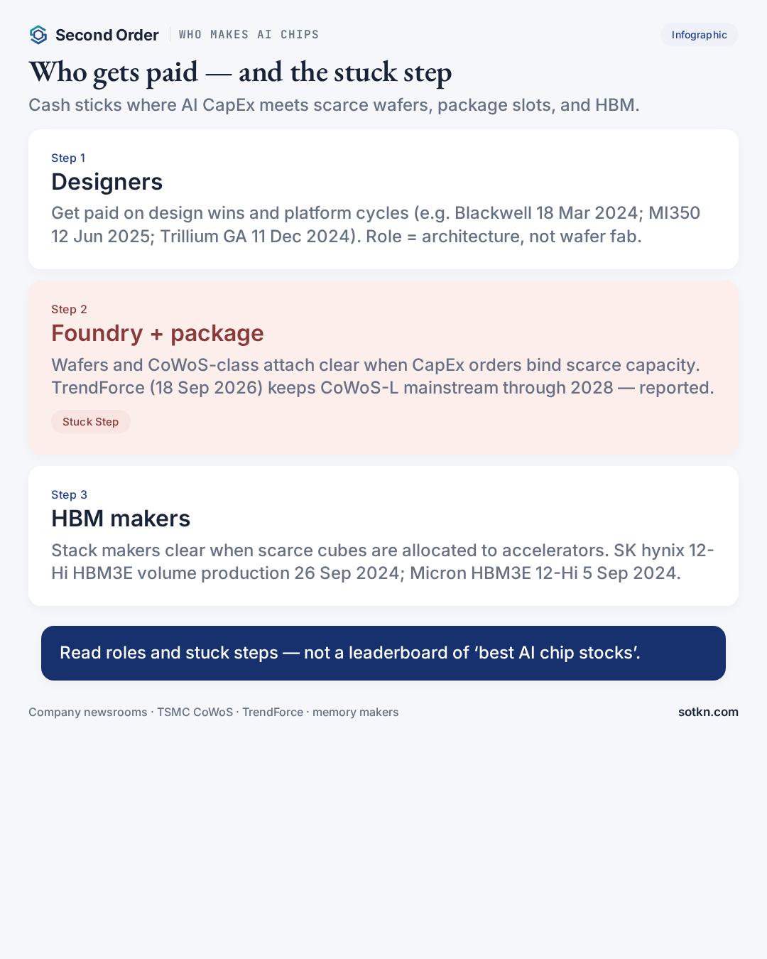
On the Semiconductors layer, who gets paid tracks which role clears first when AI CapEx orders arrive. Designers clear on wins; foundries clear when advanced wafers bind; packaging clears when CoWoS-class slots bind; HBM makers clear when scarce cubes are allocated. The stuck step is usually foundry plus packaging plus HBM together — orders can rise while installs wait.
Korea markets door where memory allocation bites: Korea HBM — who gets paid when AI memory stays scarce. Wire on the packaging clock: CoWoS-L stays the packaging path through 2028. Analysis on where the bind moves next: If packaging catches up, where does the stuck step move?.
Common misconceptions
- People assume “who makes AI chips” means one company. Actually four roles share the chain: designers, foundries, packaging attach, and HBM makers. Missing any one role leaves the accelerator waiting.
- People assume the designer also fabricates the wafer and the HBM cube. Actually most leading AI GPUs are designed by one firm, fabricated at a foundry, packaged with HBM from memory makers. Roles are separate even when brands appear on one board.
- People treat a market-share table as a tip sheet. Actually this page maps roles and stuck steps. Share prints from trade press are labelled reported and are not buy/sell advice.
- People assume packaging is just assembly after the “real” chip is done. Actually CoWoS-class attach is often the short clock. TrendForce (18 Sep 2026) keeps CoWoS-L mainstream through 2028 — reported — because package size and HBM count keep rising.
FAQ
Who makes AI chips?
AI chips are made across four roles: accelerator designers (GPU/ASIC), foundries that fabricate logic wafers, advanced-packaging partners that attach logic beside HBM, and HBM stack makers. This is a roles map, not a stock tip sheet.
Who designs AI GPUs and ASICs?
Accelerator designers own the architecture and software stack. NVIDIA announced the Blackwell platform on 18 March 2024 and Blackwell Ultra (GB300 NVL72) on 18 March 2025 (NVIDIA Newsroom). AMD unveiled Instinct MI350 Series on 12 June 2025 (AMD IR). Hyperscaler custom ASICs — e.g. Google Trillium TPU GA on 11 December 2024 (Google Cloud Blog) — sit in the same designer role.
Who fabricates AI chip wafers?
Foundries fabricate the logic dies on advanced nodes. Most leading AI GPUs and many ASICs are built at TSMC; packaging then attaches HBM on CoWoS-class platforms (TSMC CoWoS page; CoWoS-L in volume since 2024).
Does packaging make the AI chip?
Packaging does not design the GPU or fabricate the DRAM cube. CoWoS-class advanced packaging integrates logic dies with HBM stacks supplied by memory makers (TSMC CoWoS). TrendForce (18 Sep 2026) keeps CoWoS-L as mainstream AI packaging through 2028 — reported research.
Who supplies HBM for AI chips?
HBM cubes come from DRAM stack makers such as SK hynix, Samsung, and Micron. SK hynix began volume production of 12-layer HBM3E on 26 September 2024; Micron shipped production-capable HBM3E 12-high units as of 5 September 2024. See Who Makes HBM for the memory roles map.
Who gets paid when AI CapEx orders bind?
Cash sticks first where capacity is scarce: advanced foundry wafers, CoWoS-class package slots, and HBM stacks. Designers clear design wins; foundries and packaging clear when wafers and attach slots bind; memory makers clear when scarce cubes are allocated.
Is this a list of the best AI chip stocks?
No. Second Order Players pages map roles and stuck steps. They do not rank tickers, give buy/sell calls, or treat market-share tables as investment advice.
Related terms
- Who Makes HBM — roles map for the memory stack chain.
- HBM — what high-bandwidth memory is.
- CoWoS — the packaging attach that sits next to HBM.
- Foundry and advanced packaging — wafer fab and package attach as one money chain.
Markets and stack doors
Layer: semiconductors. Markets: Korea HBM memory.
Further reading
Wire: CoWoS-L through 2028 — packaging still binds. Analysis: where the stuck step moves if packaging catches up.
Get the Wire — short notes when foundry, packaging, or HBM clocks move.
How we check this
Figures come from company filings and government releases, each dated in the list below. Capacity and timing from press reports are labelled as reported, not guided. Where we work something out ourselves, the arithmetic is shown in full.
Last reviewed: 25 Sep 2026 · Next review: after next major foundry/packaging/HBM capacity note
Spot an error? Tell us and we will correct it and note the change here.
Sources
- NVIDIA Newsroom — Blackwell platform / GB200 Grace Blackwell Superchip & GB200 NVL72 (18 Mar 2024)
- NVIDIA Newsroom — Blackwell Ultra / GB300 NVL72 & HGX B300 (18 Mar 2025)
- AMD IR — Instinct MI350 Series unveiled at Advancing AI (12 Jun 2025)
- Google Cloud Blog — Trillium (6th-gen TPU) general availability (11 Dec 2024)
- TSMC — CoWoS integrates SoCs and HBM stacks; CoWoS-L volume since 2024 (accessed 25 Sep 2026)
- TrendForce — CoWoS-L mainstream AI packaging through 2028 (18 Sep 2026, reported research)
- SK hynix Newsroom — volume production of 12-layer HBM3E 36 GB (26 Sep 2024)
- Micron — HBM3E 12-high 36 GB; >1.2 TB/s; CoWoS / OSAT collaboration note (5 Sep 2024)