
Who Makes Wafer Fab Equipment? The Five Toolmakers Behind AI Chips
Wafer fab equipment is the set of machines that turn blank silicon into chips. Five toolmakers sell most of it. They are paid before a fab makes its first wafer. The EUV scanner is the tightest tool.
EXPLAINED · Players · Last reviewed: 09 Oct 2026 · Next review: after ASML Q3 2026 results (14 Oct 2026) and Lam, KLA and Applied results
Wafer fab equipment (WFE) is the set of machines a chip factory uses to turn blank silicon wafers into finished chips: lithography, deposition, etch, cleaning and inspection tools.
In short. Wafer fab equipment is the set of machines that turn blank silicon into chips. Five toolmakers sell most of it: ASML, Applied Materials, Lam Research, Tokyo Electron and KLA. SEMI expects WFE sales to rise 23.1% to $143.9 billion in 2026, with memory for AI growing fastest. Toolmakers are paid before a fab makes its first wafer. The stuck step is the EUV scanner: one maker, about 65 systems of capacity this year.
Why an investor cares: every AI chip starts as a fab full of tools. The toolmakers are paid when those tools ship, years before the chips earn anything. For the chips themselves, see who makes AI chips.
Who makes wafer fab equipment?
Five companies sell most of it. Each owns a different set of steps. A chip goes through hundreds of steps, and many repeat layer after layer.
| Toolmaker | What its tools do | Latest dated print |
|---|---|---|
| ASML (Netherlands) | Lithography: prints the chip pattern with light. Only maker of EUV scanners | Q2 2026 sales €9.3B; 86 new systems sold (15 Jul 2026) |
| Applied Materials (US) | Widest range: deposition, etch, implant, polishing, some inspection | Chip-tool revenue $7.04B in quarter to 26 Jul 2026, up 27% (13 Aug 2026) |
| Lam Research (US) | Etch and deposition, including the deep etch for 3D memory | Revenue $6.72B in quarter to 28 Jun 2026, a record (29 Jul 2026) |
| Tokyo Electron (Japan) | Coater/developers that work beside the scanner, plus etch, deposition and cleaning | Sales ¥732.4B in Apr–Jun 2026, up 33.3% (30 Jul 2026) |
| KLA (US) | Inspection and measurement: finds defects layer by layer | Revenue $3.66B in quarter to 30 Jun 2026 (28 Jul 2026) |
Sources: company results releases, July–August 2026. Roles are what each company is best known for, not a full product list or a market-share ranking.
Think of it as print, build, carve and check. ASML prints the pattern. Applied Materials, Lam Research and Tokyo Electron build up and carve away the layers. KLA checks the work.
What does each toolmaker do?
ASML makes lithography scanners. They shine light through a mask to print the chip’s pattern on the wafer. It is the only company that makes EUV (extreme ultraviolet) scanners, which the most advanced chips need. In the second quarter of 2026 it sold 86 new systems and had €9.3 billion in sales. See who makes EUV machines.
Applied Materials has the widest range. Its tools lay down thin films (deposition), etch them, implant atoms and polish layers flat. Its chip-tool business had $7.04 billion of revenue in the quarter to 26 July 2026. Foundry and logic customers were 67% of that, and DRAM 26%, up from 22% a year earlier.
Lam Research is the etch and deposition specialist. Its tools carve the very deep holes used to stack memory cells. It had record revenue of $6.72 billion in the quarter to 28 June 2026 and guided to $8.10 billion for the next quarter.
Tokyo Electron makes the coater/developer tracks that sit beside every scanner, coating wafers before printing and developing them after. It also sells etch, deposition and cleaning tools. Its sales rose 33.3% to ¥732.4 billion in April to June 2026.
KLA makes inspection and measurement tools. They find defects and check that each layer is the right size, so a bad wafer is caught before more money goes into it. KLA had $3.66 billion of revenue in the quarter to 30 June 2026.
How big is the wafer fab equipment market?
SEMI, the industry association, forecast on 14 July 2026 that WFE sales will rise 23.1% to $143.9 billion in 2026. That follows a record $116.9 billion in 2025. It expects 21.8% more growth in 2027 and about $200 billion in 2028.
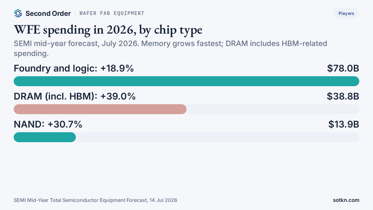
Foundry and logic is the biggest slice at $78.0 billion, up 18.9%, driven by AI accelerators. DRAM grows fastest, up 39.0% to $38.8 billion. SEMI says that is driven by HBM-related spending. HBM is the stacked memory that sits beside every AI chip. See what HBM is.
Who gets paid first?
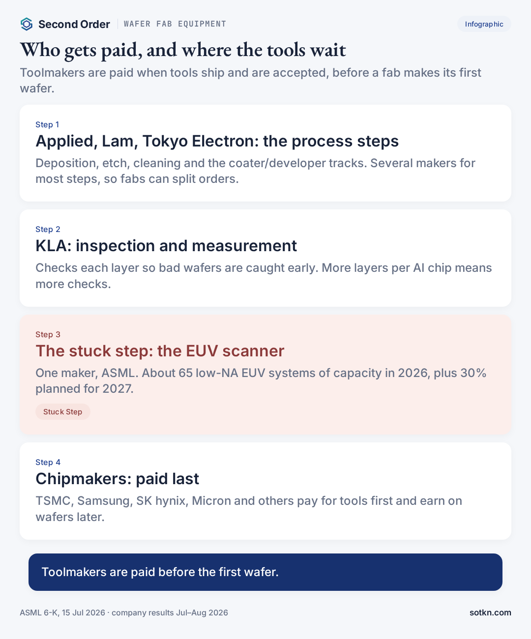
The toolmakers. A chipmaker orders tools, takes delivery and pays for them before the fab makes its first sellable wafer. The chipmaker earns its money back over years of wafers. The toolmaker has already been paid.
That is why toolmaker guidance moves before chip output does. All five expect a bigger next quarter. Here is how big, on their own guidance:
| Maker | Last qtr | Guide (mid) | Move |
|---|---|---|---|
| ASML | €9.33B | €11.5B | +23% |
| Applied (total) | $9.12B | $10.25B | +12% |
| Lam | $6.72B | $8.10B | +21% |
| KLA | $3.66B | $4.0B | +9% |
| TEL | ¥732B | ~¥888B | +21% |
Sources: company releases, July–August 2026. Guide is the midpoint of each company’s range (ASML €11.0–12.0B, Applied ±$0.5B, Lam ±$0.4B, KLA ±$0.2B); TEL’s is implied. Move is against last quarter, rounded, our arithmetic. TEL is Tokyo Electron. Tokyo Electron gives a half-year forecast of ¥1.62 trillion; ¥1,620.0B − ¥732.4B = ¥887.6B for July–September, our arithmetic.
Read those numbers as orders turning into shipments, not as chips sold. A chipmaker’s capex is the toolmakers’ revenue. For the cash side, see what cash capex is.
Where is the stuck step in wafer fab equipment?
The EUV scanner. For most process steps a chipmaker can choose between two or three toolmakers and split its orders. For EUV there is one supplier.
ASML said on 15 July 2026 that its 2026 capacity is around 65 low-NA EUV systems. It plans to add 30% for 2027, and is looking at another 30% for 2028. That is about 85 systems in 2027 and about 110 in 2028 if both steps happen (our arithmetic). Every leading-edge logic fab and every advanced DRAM fab competes for those slots.
There is a second wait: space. A tool needs a finished clean room to go into. When the building is late, the tool waits. See our Micron clean-room analysis.
What to check next
ASML’s third-quarter 2026 results are scheduled for 14 October 2026. Check sales against its €11.0–12.0 billion guide, and any update on EUV capacity for 2027. Lam, KLA and Applied report later in October and November; their dates were not all confirmed as of 9 October. Then watch SEMI’s year-end forecast in December against $143.9 billion.
Common misconceptions
- People assume chipmakers build their own tools. Actually they buy them. TSMC, Samsung, SK hynix and Micron are the customers.
- People assume ASML is the whole story. Actually lithography is one of many steps. Applied’s chip tools, Lam and KLA alone took in $17.4 billion last quarter (our sum), well above ASML’s €9.3 billion.
- People assume tool orders mean chips are already made. Actually tools are paid for first. Chips come months or years later.
- People assume all tools are equally scarce. Actually most steps have several suppliers. EUV has one.
FAQ
What is wafer fab equipment?
Wafer fab equipment (WFE) is the set of machines a chip factory uses to turn blank silicon wafers into chips: lithography, deposition, etch, cleaning and inspection tools. SEMI’s figure also counts mask and fab facility equipment.
Who makes wafer fab equipment?
Five companies sell most of it: ASML (lithography), Applied Materials (deposition, etch and more), Lam Research (etch and deposition), Tokyo Electron (coater/developers, etch, deposition and cleaning) and KLA (inspection and measurement).
How big is the wafer fab equipment market?
SEMI forecast on 14 July 2026 that WFE sales will rise 23.1% to $143.9 billion in 2026, after a record $116.9 billion in 2025, and reach about $200 billion in 2028.
Why does AI drive wafer fab equipment spending?
AI chips need leading-edge logic and high-bandwidth memory (HBM). Both take more steps and more tools per wafer. SEMI expects DRAM equipment, which includes HBM-related spending, to grow fastest in 2026, up 39.0% to $38.8 billion.
Where is the stuck step in wafer fab equipment?
The EUV scanner. ASML is the only maker and says its 2026 capacity is around 65 low-NA EUV systems. It plans to add 30% for 2027. A fab can buy other tools from several makers, but not EUV.
Is this a list of stocks to buy or sell?
No. Second Order Explained pages explain who does what and how the money moves. They do not give buy or sell calls.
Related terms
- EUV lithography — how the pattern is printed.
- Who makes EUV machines — ASML and its suppliers.
- Who makes HBM — the memory makers buying DRAM tools.
- Hybrid bonding — the next tool step for stacked chips.
Stack doors
Layer: Semiconductors. Markets: Samsung’s ₩107 trillion quarter. Wire: TSMC September sales.
Get the Wire — short daily notes when toolmaker guidance, EUV capacity or chip prints move.
How we check this
Figures come from each toolmaker’s own results release, filed with the SEC or published by the company, and from SEMI’s July 2026 equipment forecast. Each is dated in the list below. Roles describe what each company is best known for; they are not market-share rankings. Where we work something out ourselves, like the change from last quarter to guidance, the arithmetic is shown. This page explains how the money moves. It does not give buy or sell calls.
Last reviewed: 09 Oct 2026 · Next review: after ASML Q3 2026 results (14 Oct 2026) and Lam, KLA and Applied results
Spot an error? Tell us and we will correct it and note the change here.
Sources
- SEMI — Mid-Year Total Semiconductor Equipment Forecast, OEM Perspective (14 Jul 2026)
- ASML — Q2 2026 results, Form 6-K exhibit, SEC (15 Jul 2026)
- Applied Materials — Q3 fiscal 2026 results, Form 8-K exhibit, SEC (13 Aug 2026)
- Lam Research — results for the quarter ended 28 Jun 2026, Form 8-K exhibit, SEC (29 Jul 2026)
- Tokyo Electron — Summary of Consolidated Financial Results, Q1 FY2027 (30 Jul 2026)
- KLA — fiscal 2026 Q4 and full-year results, Form 8-K exhibit, SEC (28 Jul 2026)