What Is an Interposer? The Silicon Sheet Under AI Chips
An interposer is the thin layer, usually silicon, that sits under an AI processor and its memory and wires them together. Every CoWoS package needs one, it is made in a wafer fab, and new supply from GlobalFoundries does not arrive until 2028.
EXPLAINED · Mechanism · Last reviewed: 17 Oct 2026 · Next review: after TSMC's fourth-quarter 2026 earnings call
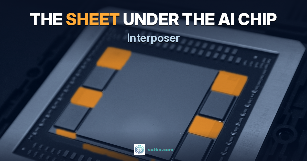
An interposer is a thin layer, usually silicon, that sits between chips and their package and wires the chips to each other far more densely than the package can. In an AI accelerator it is the sheet the processor and its high-bandwidth memory both sit on.
In short. An interposer is the thin sheet, usually silicon, that an AI processor and its high-bandwidth memory both sit on. It carries thousands of short wires between them and passes power and signals down to the package. TSMC's silicon version, used in CoWoS-S, can reach about 2,700 square millimetres; bigger packages switch to bridges inside an organic layer. Because interposers are made in wafer fabs, they are a capacity line of their own: GlobalFoundries' $2 billion deal with TSMC adds a US source, but not before the first half of 2028.
Why an investor cares: an AI chip is not finished until it is packaged, and the interposer is the piece of the package that is made in a wafer fab, with its own capacity, its own suppliers and its own lead time. When TSMC says packaging is tight, part of what is tight is this sheet. This page sits underneath how CoWoS works and what HBM is, and explains the layer that joins them.
What is an interposer?
A layer of wiring that sits between chips and the package they are mounted on. The chips on top talk to each other through it, and it passes their power and signals down to the package below.
It exists because the package itself cannot wire densely enough. An ordinary package substrate is a layered board built for connections spread out at the scale of a circuit board. An AI processor and its memory need thousands of connections packed into a few millimetres of edge. The interposer is built at chip scale, so it can carry them.
Most interposers in AI chips are silicon. TSMC describes its CoWoS-S interposer as wafer-level system integration with high-density interconnects over a large silicon area, which in plain words means the wiring is made the way chips are made, on a wafer, in a fab.
How does a silicon interposer work?
Think of it as a flat sheet with two kinds of wiring. Across the top runs fine copper wiring that joins one chip to its neighbour, such as a processor to a memory stack. Down through the sheet run vertical holes filled with metal, called through-silicon vias, that carry power and signals to the package substrate underneath.
TSMC’s small silicon bridges in CoWoS-L, which use the same wiring as CoWoS-S, carry copper lines finer than a micrometre in several layers. Its organic alternative in CoWoS-R has a minimum pitch of 4 micrometres. That gap is the reason silicon is used where the connections are densest.
Many interposers also carry built-in capacitors, small stores of charge that steady the power supply when a processor’s demand jumps. TSMC calls them embedded deep trench capacitors. GlobalFoundries named the same part in its 8 October 2026 deal with TSMC, and UMC has made interposers with them its starting point in advanced packaging.

Why do AI chips need an interposer?
Because their memory has to sit right beside the processor. High-bandwidth memory, or HBM, is a stack of memory chips placed millimetres from the processor and joined to it through very wide connections. The interposer is what makes that join possible; HBM vs GDDR shows what the wide connection buys.
Nvidia’s data-centre GPUs have sat on TSMC interposers for a decade. TSMC lists Nvidia’s Tesla P100 of 2016 among its CoWoS products. In January 2025 Nvidia’s chief executive, Jensen Huang, said its Hopper chips use CoWoS-S and that Blackwell would largely use CoWoS-L, which adds silicon bridges inside a larger organic interposer, and that the shift was to increase capacity, not reduce it.
The newer AI accelerators join more than one processor die as well as memory, which needs more area. That is where the different kinds of interposer come in. The table below sets them side by side, and CoWoS vs EMIB compares TSMC’s route with Intel’s.
| Type | What it is made of | Dated example |
|---|---|---|
| Silicon interposer | A slice of silicon wafer with fine copper wiring on top and through-silicon vias down through it | TSMC CoWoS-S, in production since 2012, up to 3.3x reticle (~2,700 mm²) |
| Organic (RDL) interposer | Layers of polymer and copper lines, cheaper and more flexible, less dense | TSMC CoWoS-R, in volume since 2023, 4 μm minimum pitch |
| RDL plus silicon bridges | An organic interposer with small silicon bridges only where chips meet | TSMC CoWoS-L, 3.5x reticle in volume since 2024; 5x in production by 15 Oct 2026 |
| No full interposer | Small silicon bridges set straight into the package substrate | Intel EMIB, in volume since 2017 |
From TSMC's CoWoS technology page and Intel's EMIB brief. Sources under References.
Why does interposer size matter?
Because the size of the sheet sets how much processor and memory fit in one package. Sizes are quoted against the reticle, the largest area a lithography tool prints in one exposure. TSMC says CoWoS-S can reach 3.3 times the reticle, or about 2,700 square millimetres, which puts one reticle at roughly 820 square millimetres (our arithmetic).
The sheet has kept growing. TSMC’s own milestone list shows a GPU on a one-reticle interposer by 2019 and a two-reticle interposer with Broadcom in March 2020. CoWoS-L at 3.5 times went into volume in 2024. On its 15 October 2026 earnings call TSMC said packages at five times the reticle were in production, with larger sizes in development.

Above 3.3 times, TSMC recommends CoWoS-L or CoWoS-R rather than one solid silicon sheet. Our read: a silicon interposer is cut from a round wafer, so the bigger each one is, the fewer fit on a wafer and the more each defect costs. Bridges inside an organic layer use silicon only where the chips meet, which is how packages keep growing without one giant piece of silicon.
Who makes interposers?
Mostly TSMC, for its own CoWoS packages. Two other foundries have stepped in as second sources, and both use older production lines, which is the unusual part: an interposer’s wiring is far coarser than a leading-edge processor’s, so a fab that no longer makes leading chips can still earn AI money making it.
UMC was reported on 31 May 2026 to have doubled its silicon interposer capacity from 3,000 to 6,000 wafers a month, mostly on 55 and 65 nanometre technology. GlobalFoundries signed a $2 billion, five-year agreement with TSMC on 8 October 2026 to make interposers, including the built-in capacitors, at its Malta, New York fab. It called this the first US source of the part. Volume is due to start ramping in the first half of 2028.
| Maker | Role | Dated fact |
|---|---|---|
| TSMC | Makes most interposers for its own CoWoS packages, in Taiwan | Said on 16 Jul 2026 that packaging capacity was so tight it was limiting customers' growth |
| UMC | Makes silicon interposers on older 55 and 65 nanometre lines | Reported 31 May 2026: interposer capacity raised from 3,000 to 6,000 wafers a month |
| GlobalFoundries | Will make silicon interposers for TSMC as a manufacturing service in Malta, New York | $2 billion, five-year deal signed 8 Oct 2026; volume ramp in the first half of 2028 |
| Intel Foundry | Avoids the full interposer with EMIB bridges in the substrate | EMIB in volume since 2017 |
Company releases, transcripts and one press report labelled as reported. Sources under References.
Who joins the finished package, after the interposer is made, is mapped in who makes advanced packaging. The GlobalFoundries deal itself is in our Wire on the $2 billion interposer deal.
Who gets paid, and where is the stuck step?
- The interposer maker, per wafer. TSMC inside its own packaging price, or UMC and, from 2028, GlobalFoundries as outside suppliers.
- The packager, for the join. Placing the processor and memory on the interposer and bonding it to the substrate is the CoWoS step, and it is where TSMC’s packaging revenue sits.
- The memory and substrate makers, alongside. Every interposer carries HBM stacks on top and needs a substrate underneath; how that layer works is in IC substrates and ABF.
- The stuck step: interposer and packaging capacity. A finished processor die that has no interposer slot waits. TSMC said on 16 July 2026 that packaging was so tight it was limiting its customers’ growth, and new outside interposer supply from GlobalFoundries lands only in 2028.
Our view: the headline number for AI packaging is CoWoS capacity, but the interposer is one of the inputs that sets it. Watch who adds interposer wafers, at what size, and when. A second source that ramps in 2028 does not ease 2026 or 2027. The capacity side is tracked in TSMC CoWoS capacity.
What would prove this wrong?
- Bridges replace whole sheets faster. If CoWoS-L and EMIB-style bridges take most new AI packages, each package uses far less silicon interposer area, and interposer wafers stop being the tight input.
- TSMC stops calling packaging tight. If the next earnings calls describe packaging capacity as balanced, the stuck step has moved somewhere else, such as memory or power.
- Outside supply arrives early. If GlobalFoundries or UMC ship interposers in volume before 2028, the second-source clock is shorter than the release implies.
What to check next
TSMC’s fourth-quarter 2026 earnings call, expected in January 2027, for any change in how tight packaging is and the next package size in production. GlobalFoundries’ third-quarter results for spending at Malta and how the $2 billion lands by year. UMC’s quarterly calls for any new interposer capacity. The wafer side of the same week is in TSMC’s third-quarter print.
Common misconceptions
- People assume the interposer is part of the chip. Actually it is a separate piece, made separately, that the chips are mounted on.
- People assume interposers need the newest fabs. Actually UMC makes them on 55 and 65 nanometre lines; the wiring is coarse by processor standards.
- People assume every AI package uses one big silicon sheet. Actually above 3.3 times the reticle TSMC recommends bridges inside an organic layer, and Intel’s EMIB skips the full interposer.
- People assume a $2 billion interposer deal adds capacity now. Actually GlobalFoundries’ volume ramp starts in the first half of 2028.
FAQ
What is an interposer?
A thin layer, usually silicon, that sits between chips and their package and wires the chips to each other. In an AI accelerator the processor and its high-bandwidth memory both sit on the interposer, which carries thousands of short connections between them and passes power and signals down to the package.
What is a silicon interposer?
An interposer made from a silicon wafer, with very fine copper wiring on top and vertical holes filled with metal, called through-silicon vias, running down through it. TSMC's CoWoS-S uses one, up to about 3.3 times the size of a standard chip exposure, or roughly 2,700 square millimetres.
Why do AI chips need an interposer?
Because high-bandwidth memory has to sit right next to the processor with far more connections than an ordinary package can route. The interposer is a short, dense bridge between them. Without it, the memory could not feed the processor fast enough.
What is the difference between a silicon interposer and an organic interposer?
A silicon interposer is cut from a wafer and carries the finest wiring. An organic or RDL interposer is built from polymer and copper layers, is cheaper and more flexible, but wires less densely. TSMC's CoWoS-R uses an RDL interposer with a 4 micrometre minimum pitch; CoWoS-L mixes RDL with small silicon bridges.
Who makes silicon interposers?
Mostly TSMC, for its own CoWoS packages. UMC makes them on older production lines and was reported in May 2026 to have doubled that capacity to 6,000 wafers a month. GlobalFoundries signed a $2 billion, five-year deal on 8 October 2026 to make them for TSMC in New York, with volume from the first half of 2028.
Does every AI chip use an interposer?
No. Intel's EMIB joins chips with small silicon bridges set into the package instead of a full interposer, and TSMC's CoWoS-L uses local bridges inside a larger RDL interposer. But the leading AI accelerators on CoWoS all sit on some form of interposer.
Is this a list of stocks to buy or sell?
No. Second Order Explained pages explain how the money moves. They do not give buy or sell calls.
Related: CoWoS; CoWoS vs EMIB; hybrid bonding; HBM; who makes advanced packaging; rack-scale AI.
Stack doors
Layer: Semiconductors. Also: Neoclouds, Hyperscalers, AI Data Centers. Markets: Taiwan, US.
Get the Wire — short daily notes when packaging capacity, interposer supply and AI chip output move.
How we check this
Interposer types, sizes and production dates come from TSMC’s CoWoS technology page and its July and October 2026 earnings calls. The GlobalFoundries deal comes from its 8 October 2026 release, and Intel’s EMIB details from its product brief. Each was re-checked on 17 Oct 2026. UMC’s interposer capacity comes from a press report of its May 2026 shareholders’ meeting and is labelled as reported. Where we work something out ourselves, such as the area of one reticle, it is labelled “our arithmetic”. This page explains how the money moves. It does not give buy or sell calls.
Last reviewed: 17 Oct 2026 · Next review: after TSMC's fourth-quarter 2026 earnings call
Spot an error? Tell us and we will correct it and note the change here.
References
- TSMC — CoWoS technology page (read 17 Oct 2026) — CoWoS-S silicon interposer up to 3.3x reticle (~2,700 mm²), in production since 2012; CoWoS-R RDL interposer since 2023, 4 μm pitch; CoWoS-L with local silicon interconnect at 3.5x reticle since 2024; deep trench capacitors; interposer milestones
- GlobalFoundries — Agreement to establish U.S.-based supply of silicon interposers for advanced AI packaging (8 Oct 2026) — $2 billion, five-year manufacturing service to TSMC at Malta, New York; deep trench capacitors; volume ramp in the first half of 2028
- Reuters — GlobalFoundries to make key AI chip component for TSMC in $2 billion deal (8 Oct 2026) — advanced packaging a major constraint on AI chip production
- TSMC — Q2 2026 earnings conference official transcript (16 Jul 2026) — packaging capacity so tight it limits customers' growth; 10–20% of 2026 capital budget to packaging, testing, masks and others
- TSMC — Q3 2026 quarterly results and earnings conference (15 Oct 2026) — 5x-reticle packages in production; larger sizes in development
- Reuters — Nvidia CEO says its advanced packaging technology needs are changing (16 Jan 2025) — Blackwell largely on CoWoS-L, Hopper on CoWoS-S
- China Times — UMC shareholders' meeting report (31 May 2026, Chinese) — UMC silicon interposer capacity raised from 3,000 to 6,000 wafers a month, as reported
- UMC — Q2 2026 earnings call transcript (Motley Fool, 7 Aug 2026) — interposer with deep trench capacitors as UMC's entry to advanced packaging
- Intel Foundry — EMIB technology brief (July 2025) — bridges embedded in the substrate instead of a full interposer
- Wikimedia Commons — AMD Fiji GPU package with GPU, HBM memory and interposer, photo by C. Spille / pcgameshardware.de, CC BY-SA 4.0 — featured image base photo