CoWoS vs EMIB: Two Ways to Join an AI GPU — and Who Gets Paid
CoWoS puts an AI GPU and HBM on a full interposer. EMIB embeds small silicon bridges in the substrate. The stuck step is still the CoWoS slot, not the second recipe.
EXPLAINED · Versus · Last reviewed: 16 Oct 2026 · Next review: after Intel’s Q3 2026 results (29 Oct 2026)
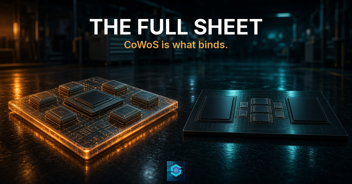
CoWoS and EMIB are two ways to join a compute die to high-bandwidth memory so an AI accelerator can ship as one module. CoWoS puts the dies on a full silicon (or hybrid) interposer, then onto a substrate. EMIB embeds small silicon bridges only where neighbouring dies need to talk, inside an ordinary organic substrate.
In short. Both routes are 2.5D packaging: they sit the GPU next to HBM instead of across a board. CoWoS, TSMC’s family, has been in volume since 2012 and is still the path most leading AI GPUs take. EMIB, Intel Foundry’s, has been in volume since 2017 and skips the full interposer. On 16 July 2026 TSMC said packaging was so tight it was limiting customer growth, and that it welcomed extra routes such as EMIB-T so front-end wafers could still become products. The stuck step is still the CoWoS-class attach slot, not the existence of a second recipe.
Why an investor cares: the two recipes carry different cheques and different clocks. CoWoS is where most shippable AI GPUs wait. EMIB is the named alternative that TSMC itself treated as overflow, not a replacement. For the CoWoS mechanism on its own, see CoWoS explained.
What is the difference between CoWoS and EMIB?
CoWoS builds a shared base — a silicon interposer, or a hybrid of redistribution layers and local silicon — then mounts the compute die and the HBM stacks on that sheet. Every signal and every power via that leaves a die has to cross that sheet. EMIB keeps a standard organic package substrate and drops a thin silicon bridge into a cavity only at the shoreline where two dies meet. The rest of the package stays ordinary flip-chip.
| CoWoS vs EMIB at a glance |
|---|
| Name: CoWoS is chip-on-wafer-on-substrate (TSMC). EMIB is Embedded Multi-die Interconnect Bridge (Intel Foundry). |
| Join: CoWoS uses a full interposer (silicon on -S; RDL or RDL-plus-local-silicon on -R and -L). EMIB embeds small silicon bridges only where links are needed. |
| In volume since: CoWoS, 2012. EMIB, 2017. |
| Who sells it: CoWoS is TSMC’s branded family. EMIB is Intel Foundry’s; Intel says it has run Intel and external silicon. |
| HBM: Both are sold as logic-to-HBM 2.5D. EMIB-T adds through-silicon vias in the bridge for vertical power, which Intel says HBM needs. |
| How big: TSMC lists CoWoS-S to about 3.3× reticle (~2,700 mm²) and CoWoS-L at 3.5× since 2024; on 15 Oct 2026 it said 5× is in production, with 9× and 14× in work. Intel’s July 2026 newsroom put New Mexico at 8× reticle today and more than 12× by 2028. |
TSMC CoWoS page (read 16 Oct 2026); TSMC Q2 2026 official transcript (16 Jul 2026); TSMC Q3 2026 earnings conference (15 Oct 2026); Intel EMIB brief (July 2025); Intel newsroom (29 Jul 2026). Size claims are the companies’ own.
The two are substitutes at the module — a finished AI GPU needs one attach recipe — and complements at the foundry. Extra attach routes, TSMC said in July, help its front-end wafer business, “which is a majority part of TSMC’s business.”
What is CoWoS?
CoWoS is TSMC’s 2.5D packaging family. A compute die and HBM stacks sit on a shared base, then that assembly sits on a substrate. Ordinary board assembly cannot put memory that close. AI GPUs need the short path so data can feed the die without waiting on distant host DRAM. The semiconductors stack is where this attach gate sits next to foundry and memory.
The family is not one process. CoWoS-S uses a silicon interposer up to about 3.3× reticle. CoWoS-R, in volume since 2023, uses an organic redistribution-layer interposer. CoWoS-L, in volume since 2024 at 3.5× reticle, mixes RDL with local silicon interconnects. TSMC recommends -L or -R when the interposer must exceed the CoWoS-S size band. A “sold out” headline usually means the scarce style the newest accelerators need — not every CoWoS line.
TSMC does not publish a CoWoS wafers-per-month figure. What is checkable from IR is CapEx intent and qualitative tightness. On 16 July 2026, about 10–20% of the US$60–64 billion 2026 capital budget was allocated to advanced packaging, testing, mask making and others — a bucket, not a pure CoWoS line item. That guide was still the one management pointed to after the 15 October print.
What is EMIB?
EMIB is Intel Foundry’s 2.5D interconnect. The July 2025 technology brief calls it the first 2.5D solution that uses bridges embedded in the substrate. The assembly flow is standard flip-chip; the difference is in how the substrate is made. Bridges sit in a cavity, held with adhesive, then dielectric and metal layers close over them. A tight microbump pitch is required only at the bridge.
That is the cost claim. A full silicon interposer makes every signal and every power via traverse the sheet. A local bridge leaves the rest of the package’s path alone. Intel says yields are comparable to a flip-chip BGA of equal complexity, and that the design has been in high volume since 2017 on server, network and HPC parts.
EMIB-M puts metal-insulator-metal capacitors in the bridge. EMIB-T adds through-silicon vias so power and high-speed I/O can pass vertically — the version Intel says HBM needs, and the one named on TSMC’s July and October 2026 calls. Combine EMIB with Foveros die-stacking and Intel calls the hybrid EMIB 3.5D. Intel’s packaging page cites the Data Center GPU Max Series: more than 100 billion transistors, 47 active tiles, five process nodes.
Intel’s 29 July 2026 newsroom note puts some of that work at Fab 9 in Rio Rancho, New Mexico: packages at 8× the industry-standard reticle today, more than 12× targeted by 2028. That is a capability claim, not a booked-slot count.
Is EMIB cheaper or better than CoWoS?
Intel’s brief says a local bridge is more cost-effective for logic-to-logic and logic-to-HBM links, because you do not pay for a full interposer wafer. TSMC does not publish a CoWoS-versus-EMIB price. There is no official “dollars per attach” series to divide.
What is checkable is the queue. On 16 July 2026, asked about EMIB-T “gaining traction,” C.C. Wei said TSMC’s packaging capacity was “so tight that now it limits my customers’ growth,” welcomed the extra flexibility, and said the competing technology “looks good, according to the newspaper.” On 15 October he said CoWoS was still “the number one choice for our customer,” that TSMC was in real-world production of 5×-reticle packages with “excellent” yield, and that if a competitor could not deliver, TSMC would support the customer as a backup.
EMIB can be cheaper per square millimetre of silicon you do not buy. It is not, on TSMC’s telling, the slot clearing the AI GPU queue. A design that starts on EMIB-T and cannot get enough attach still needs a CoWoS version — a second queue, not a substitute that removes the first.
Who gets paid — and where is the stuck step?
The money moves in a set order. The attach recipe decides who cashes the last cheque before a GPU can ship.
- The chip designer pays first. A GPU or ASIC vendor reserves packaging as well as wafers. If the attach slot is late, finished modules slip even when the die looks fine. See who makes AI chips.
- TSMC is paid for CoWoS. The branded family, and the dominant share of leading AI attach, sit at TSMC. About 10–20% of the US$60–64 billion 2026 CapEx bucket goes to packaging, testing, mask making and others. TSMC is also building 13 leading-edge and advanced-packaging fabs in Taiwan over the next several years. Markets door: TSMC CoWoS capacity.
- Intel Foundry is paid for EMIB. The cheque is for the substrate-plus-bridge flow, and for EMIB 3.5D when Foveros stacks sit on those bridges. Markets door: US.
- OSATs take overflow. ASE (including SPIL) and Amkor sell CoWoS-class or CoWoS-like attach under other names. See who makes advanced packaging.
- HBM makers wait on the same join. If packaging is late, stacks sit. If HBM is late, a reserved slot may slip. Neighbouring clock: HBM explained and the Korea hub.
The stuck step is the CoWoS-class attach slot. TSMC said so in July. In October it said CoWoS was still the first choice and that TSMC would take backup demand if a competing recipe fell short. Land notices are a permission gate, not working yields. A second recipe only moves the stuck step when it ships enough finished modules that the CoWoS queue shortens.
Hyperscaler CapEx and neocloud fleet growth show up here with lag — hyperscalers, neoclouds. If packaging eases, the stuck step can move: Where does the stuck step move?.
What would prove this wrong?
- EMIB-T takes a named leading AI GPU in volume. If a top accelerator ships its high-volume SKU on EMIB rather than CoWoS, the attach cheque splits and the CoWoS slot is no longer the only finish line.
- TSMC says packaging is no longer limiting growth. A later earnings call that drops the tightness language, without a matching fall in wafer demand, would mean the bind has moved.
- CoWoS-L / 5×-reticle yield breaks. If the large-reticle path TSMC is already running fails to hold yield, effective slots fall even as nameplate capacity rises.
What to check next
Intel reports third-quarter results on Thursday 29 October 2026, after the US close, with a call at 14:00 Pacific. Look for any named foundry packaging volume, EMIB-T customer language, and whether New Mexico is talked about as slots or as capability. On the TSMC side, the next CoWoS tell is still qualitative tightness versus the 10–20% packaging-and-other CapEx bucket — and whether 5×-reticle stays in the “real-world production” tense. Our Wire on TSMC’s Q3 print shows the wafer side of the same week.
Common misconceptions
- People assume CoWoS and EMIB are the same process with two brand names. Actually CoWoS uses a full interposer (silicon or hybrid). EMIB embeds small bridges in an organic substrate and skips the sheet.
- People assume a second recipe ends the CoWoS shortage. Actually TSMC said in July that extra routes help its front-end wafers ship, and in October that CoWoS was still the first choice — and that TSMC would take backup demand if the other recipe fell short.
- People assume a reticle-multiple headline is a capacity number. Actually 5×, 8× or 14× is how large one package can be. It is not wafers per month, and it is not a booked queue. Intel’s brief says EMIB has run Intel and external silicon since 2017 — a capability claim, not a count of AI GPU slots.
FAQ
What is the difference between CoWoS and EMIB?
CoWoS puts a compute die and HBM on a full interposer, then onto a substrate. EMIB embeds small silicon bridges in an organic substrate only where neighbouring dies need a dense link.
What is CoWoS?
CoWoS is chip-on-wafer-on-substrate — TSMC’s 2.5D packaging family, in volume since 2012, that joins a compute die to HBM so an AI GPU can ship as one module.
What is EMIB?
EMIB is Embedded Multi-die Interconnect Bridge — Intel Foundry’s 2.5D packaging, in volume since 2017, that joins dies with silicon bridges set into the package substrate.
Is EMIB cheaper than CoWoS?
Intel says a local bridge is more cost-effective than a full silicon interposer because you do not pay for the whole sheet. TSMC does not publish a CoWoS-versus-EMIB price, and it still calls CoWoS the customers’ first choice.
Who makes CoWoS and EMIB?
CoWoS is TSMC’s branded family. EMIB is Intel Foundry’s. OSATs such as ASE and Amkor sell related 2.5D attach under other names.
Is this a list of stocks to buy or sell?
No. Second Order Explained pages explain how the money moves. They do not give buy or sell calls.
Related terms
- CoWoS — the mechanism this Versus sits on.
- Who makes advanced packaging — OSAT houses versus captive attach.
- Hybrid bonding — copper-to-copper joins inside some stacks.
- HBM — the memory twin that has to arrive with the die.
- EUV vs DUV — the lithography Versus one step upstream.
Markets and stack doors
Layer: Semiconductors. Also: Hyperscalers, Neoclouds. Markets: Taiwan, TSMC CoWoS capacity, Korea, US.
Get the Wire — short daily notes when chip tools, memory and capacity move.
How we check this
Process descriptions and dates come from TSMC’s and Intel’s own technology pages, filings and earnings conferences, listed under Sources. Each was re-checked on 16 Oct 2026. TSMC’s 15 October remarks on 5×-reticle production are from the public earnings conference; the official written transcript had not been posted on TSMC IR at review. Capacity in wafers per month is not an official TSMC figure and is not used here. This page explains how the money moves. It does not give buy or sell calls.
Last reviewed: 16 Oct 2026 · Next review: after Intel’s Q3 2026 results (29 Oct 2026)
Spot an error? Tell us and we will correct it and note the change here.
Sources
- TSMC — CoWoS technology page (read 16 Oct 2026)
- TSMC — Q2 2026 earnings conference official transcript (16 Jul 2026)
- TSMC — Q3 2026 Earnings Release (15 Oct 2026)
- TSMC — Q3 2026 quarterly results page (read 16 Oct 2026)
- TSMC — Q3 2026 earnings presentation (15 Oct 2026)
- Intel Foundry — EMIB technology brief (July 2025)
- Intel Foundry — Advanced packaging page (read 16 Oct 2026)
- Intel — U.S. advanced packaging newsroom note (29 Jul 2026)
- Intel — Q3 2026 results date (6 Oct 2026)
S
Writes Second Order by TKN — a plain-English map of AI infrastructure and semiconductors for non-specialist investors. Focus: who gets paid, where money sticks, and which step is stuck.