
What Is a 2nm Chip? Gate-All-Around Transistors, Explained
A 2nm chip is built on a foundry's newest process, where the transistor gate wraps all the way around stacked silicon sheets. TSMC's 2nm was 8% of its wafer revenue in the third quarter of 2026; capacity, not the design, is the stuck step.
EXPLAINED · Mechanism · Last reviewed: 1 Nov 2026 · Next review: after TSMC’s October sales (10 Nov 2026), Applied Materials’ results (12 Nov 2026) and TSMC’s fourth-quarter results in January 2027
A 2nm chip is a chip made on a foundry’s 2-nanometer-class process, the first generation to use gate-all-around transistors, where the gate wraps around stacked silicon sheets instead of three sides of a fin.
In short. A 2nm chip is made on a foundry’s newest process, where the transistor gate wraps all the way around stacked silicon sheets instead of three sides of a fin. The name is a label, not a measurement. TSMC says its N2 uses 25–30% less power than its 3nm N3E for the same speed, and 2nm was already 8% of its wafer revenue in the third quarter of 2026. Our read: toolmakers are paid first, TSMC is paid per wafer but pays for the ramp in margin, and the stuck step is capacity, meaning cleanroom space and tools, not the transistor design.
Why an investor cares: the newest node is where the best-paid chips are made, and where the scarcest factory space sits. AI accelerators, server processors and flagship phones all queue for it. Our guide to who makes AI chips covers the designers; this page covers the process they are queuing for.
What is a 2nm chip?
A 2nm chip is a chip made on a foundry’s 2-nanometer-class process. At TSMC that is N2 and its later versions, N2P and A16. At Intel it is 18A. Each is a full set of manufacturing steps, from the transistors at the bottom of the chip to the copper wiring on top.
What sets this generation apart is the transistor. TSMC’s N2 is the first TSMC node to use gate-all-around, or nanosheet, transistors. Intel’s 18A does the same with what it calls RibbonFET. That is the first change in the basic transistor shape at the leading edge since FinFETs arrived about 15 years ago.
The chip itself looks like any other once it is packaged. An AI accelerator built on 2nm still needs memory beside it and packaging around it. Our guide to chiplets covers how dies on different nodes are combined in one package.
Is anything on a 2nm chip 2 nanometers wide?
No, and that surprises most people. Node names began as the length of the transistor gate. From the mid-1990s chipmakers shrank some features faster than others, and the names kept counting down on the old schedule.
IEEE Spectrum reported in 2020 that the node number had not matched any physical feature for about two decades. When Intel moved to FinFETs at its 22nm node in 2011, the transistors had 26nm gates and a 40nm half-pitch, the half-distance between wires.
Read 2nm as a generation label. It tells you the process is newer and denser than 3nm, not that any part measures two nanometers. That is also why one company’s 2nm cannot be compared directly with another’s by name alone.
What is a gate-all-around transistor?
A transistor is a switch. Current flows through a channel from one end to the other, and a gate above it turns the flow on and off. The more of the channel the gate touches, the better it controls the current and the less leaks out when the switch is off.
| Transistor | Where the gate touches the channel | Used at |
|---|---|---|
| Planar | One side, from the top of a flat channel | Older nodes, before FinFETs |
| FinFET | Three sides of a vertical silicon fin | About 22nm to 3nm (Intel from 2011; TSMC to N3) |
| Gate-all-around (nanosheet) | All four sides of stacked horizontal silicon sheets | Samsung 3nm (2022), Intel 18A, TSMC N2 (2025) and beyond |
Each company has its own name for gate-all-around: nanosheet (TSMC), MBCFET (Samsung) and RibbonFET (Intel). Dates are company statements.
In a planar transistor the gate sat on top of a flat channel. In a FinFET the channel stands up as a thin fin and the gate wraps three sides. In a gate-all-around transistor the channel is a stack of thin horizontal silicon sheets, and the gate wraps all four sides of each one.
Two things follow. Leakage falls, because the gate grips the whole channel. And designers can choose the width of the sheets, trading speed against power for each block of the chip. Samsung, which began gate-all-around production at 3nm in June 2022, made the same point about adjustable sheet width in its launch release.
How much better is 2nm than 3nm?
On the companies’ own numbers, it is a meaningful step in power and a modest one in density. TSMC says N2 is 10–15% faster at the same power, or uses 25–30% less power at the same speed, than N3E, its main 3nm process. Its N2P version, which TSMC expects to be most of its 2nm business, raises that to 18% faster or 36% less power.
| Process | Faster at the same power | Less power at the same speed | Chip density | Compared with |
|---|---|---|---|---|
| TSMC N2 | 10–15% | 25–30% | About 1.15× | TSMC N3E |
| TSMC N2P | 18% | 36% | 1.15× | TSMC N3E |
| TSMC A16 | 8–10% | 15–20% | Up to 1.10× | TSMC N2P |
| Intel 18A | Up to 15% better performance per watt | 30% better | Intel 3 | |
| Samsung 3nm GAA (first generation) | 23% higher performance | Up to 45% | 16% smaller area | Samsung 5nm |
Company claims from TSMC (its technology pages, checked 1 Nov 2026, and its April 2025 symposium figures as reported by Tom’s Hardware), Intel (October 2025) and Samsung (June 2022). Each compares with its own earlier process, so do not rank one company’s numbers against another’s.
Density is the surprise. TSMC quotes N2 at about 1.15 times the chip density of N3E, measured on a mix of 50% logic, 30% memory and 20% analog circuits. Our arithmetic: a classic full-node shrink, 30% smaller in both directions, roughly doubles density, since 0.7 × 0.7 is about 0.5 of the area. So 2nm is a power node first and a shrink node second.
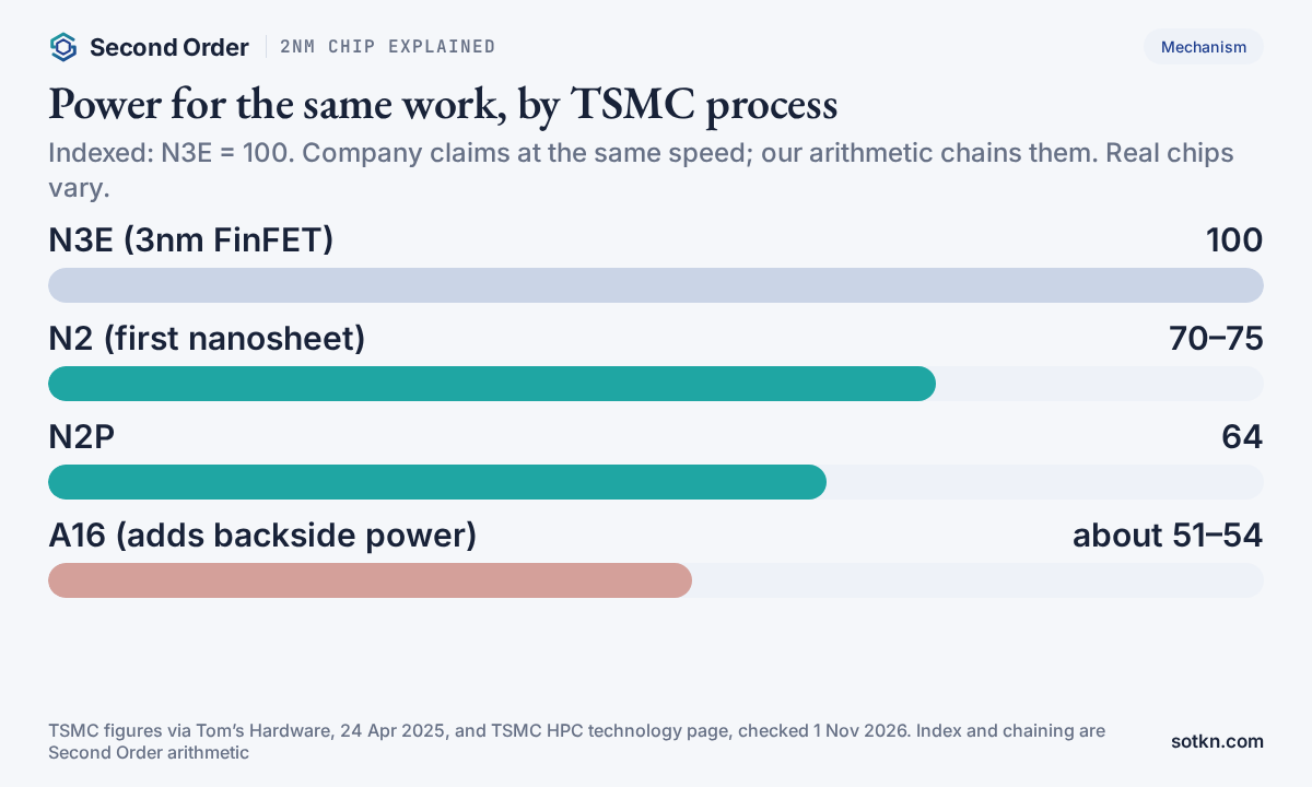
Our arithmetic, chaining TSMC’s claims at the same speed: if a block of logic draws 100 units of power on N3E, it draws 70–75 on N2 and 64 on N2P. A16 claims another 15–20% less than N2P, which takes it to about 51–54. Real chips will not hit those numbers exactly, because each claim is measured on a reference design under set conditions.
What is backside power, and why does it come next?
Today a chip’s power wires and signal wires share the same crowded layers above the transistors. Backside power moves the power wiring under the transistors, to the back of the wafer, leaving the front for signals. Less voltage is lost on the way in, and the signal wiring has more room.
Intel ships it now: 18A combines RibbonFET transistors with PowerVia backside power, and Intel said in October 2025 that its Panther Lake processors on 18A were in production at Fab 52 in Arizona. TSMC’s version, Super Power Rail, arrives with A16, which TSMC targets at high-performance computing.
TSMC’s chairman, C.C. Wei, said on the October 2026 call that whether a customer uses backside power depends on the product: some accelerators might, while phones do not. Our read: backside power is an AI and server option, not a step every 2nm customer will take.
Who makes 2nm chips in 2026?
TSMC is the volume leader. It says N2 entered high-volume manufacturing in the fourth quarter of 2025 with good yield, and is ramping in phases at its Hsinchu and Kaohsiung sites in Taiwan. It expects N2 family capacity to more than double in 2027, on demand from both smartphones and AI computing.
Intel makes 18A for its own processors in Arizona. Samsung was first to use gate-all-around in production, at its 3nm node in 2022. AMD said in April 2025 that its next EPYC server processor, Venice, was the first high-performance product brought up on TSMC N2. Our TSMC Stack page covers how the foundry fits into the AI chip chain.
The numbers are already visible in TSMC’s results. In the third quarter of 2026, 2nm was 8% of its wafer revenue and 3nm was 33%. Our arithmetic: the two newest nodes made up 41% of wafer revenue. Our Catalyst note on TSMC’s third quarter covers the full print.
Our arithmetic gives a ceiling on the dollars: 8% of TSMC’s US$46.72 billion of total quarterly revenue is about US$3.7 billion. Wafer revenue is smaller than total revenue, so 2nm wafer sales were below that figure. TSMC does not publish the exact amount.
Who gets paid as 2nm ramps?
The order matters more than the total. Money for a new node is spent years before a 2nm chip lands in a data centre, and the people paid first are not the people who sell the chip.
| Who | When they are paid | What the 2026 numbers say |
|---|---|---|
| Toolmakers (Applied Materials, Lam Research, Tokyo Electron, KLA, ASML) | First, when tools ship into a new fab | Applied said gate-all-around and FinFET capacity additions drove record foundry-logic revenue in its quarter to July 2026 |
| Foundry (TSMC, Intel, Samsung) | Per wafer, once output starts | 2nm was 8% of TSMC wafer revenue in Q3 2026, but cut its gross margin by 1.3 points as the line ramped |
| Chip designers (AMD, Apple, AI accelerator makers) | When finished chips ship, after paying for wafers | AMD’s Venice server CPU was the first high-performance product brought up on TSMC N2, due in 2026 |
| Data centre operators | Last, through lower power per unit of work | Same work on 25–36% less chip power on TSMC’s N2 and N2P figures versus N3E |
Order and timing are our read; figures are from the companies’ 2025–2026 releases, filings and calls listed under References.
Toolmakers are paid first. In February 2026 Applied Materials launched new deposition, etch and treatment systems aimed at gate-all-around transistors at 2nm and beyond: one smooths the silicon sheets, one etches the trenches between them, and one swaps tungsten contacts for molybdenum. In August it said capacity additions in gate-all-around and FinFET drove record foundry-logic revenue. Our guide to who makes wafer fab equipment maps who sells which tools.
Our arithmetic on Applied’s own guide: Semiconductor Systems revenue of about US$7.0 billion in the quarter to July and a guide of about US$7.9 billion for the quarter to October is a step of roughly 13% in one quarter. Applied reports on 12 November 2026.
The foundry is paid per wafer, but a new node costs money before it makes money. TSMC said its third-quarter gross margin fell 1.3 points to 66.4%, mainly because of the early 2nm ramp. Our arithmetic: that implies about 67.7% in the second quarter. It guided the fourth quarter down again, to 66% at the midpoint, citing the steep 2nm ramp and its overseas fabs.
Chip designers pay for wafers and are paid when chips ship. The buyer at the end, the data centre, is paid last, in lower power bills for the same work. Applied’s chief executive put it plainly in August: AI data centre returns depend on tokens per second and total cost of ownership, which is dominated by energy. Our guide to how much power an AI data centre uses shows why that matters.
Where is the stuck step?
Our read: in capacity, not in the transistor. TSMC says N2 is yielding well. What it cannot do fast enough is add output. On the October call it said demand is still higher than supply after checking customers’ data centre and power plans, and that tool supply is tight.
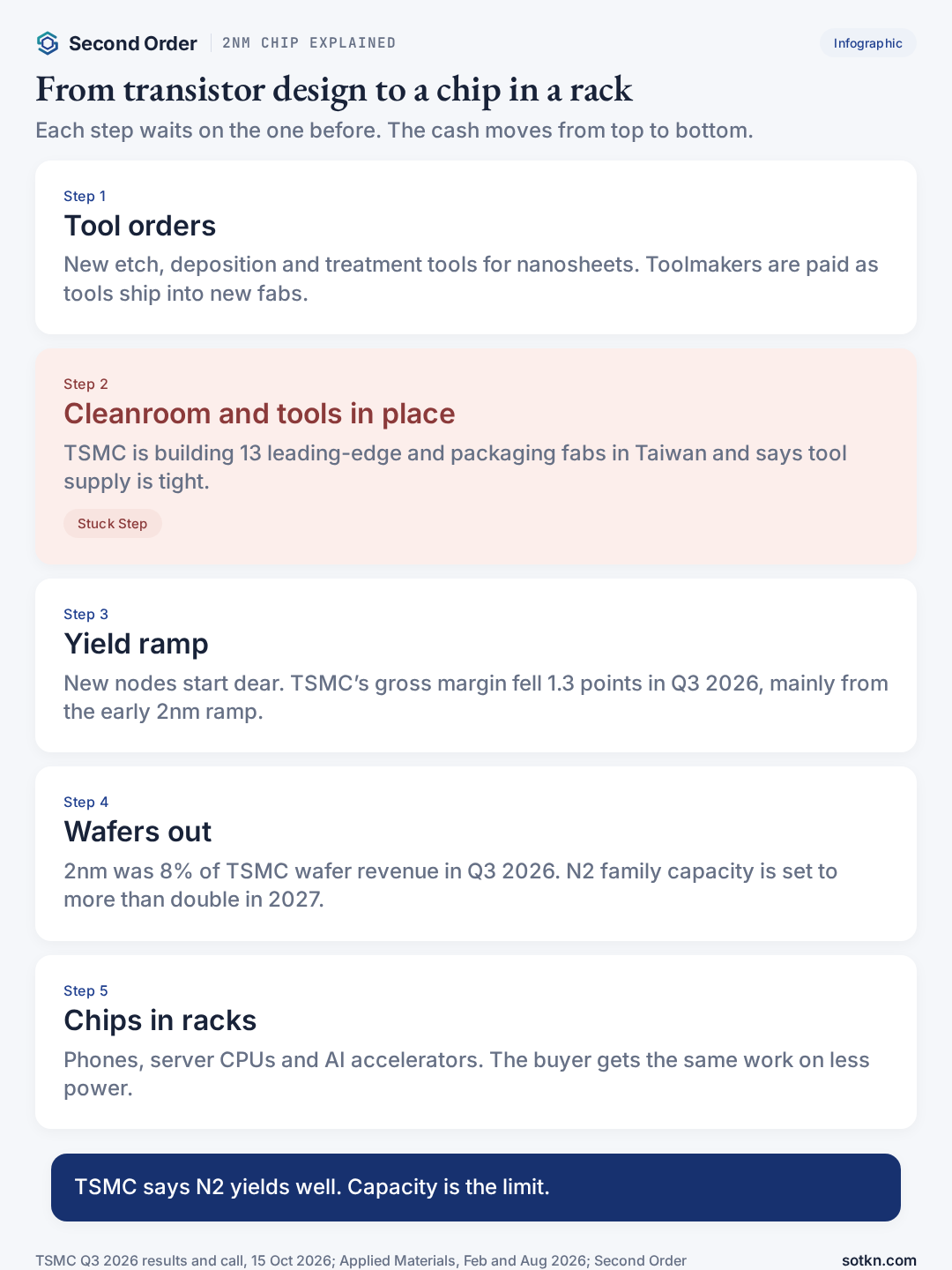
The physical limit is cleanroom space and the tools to fill it. TSMC says it has nearly 20 fabs in progress worldwide, including 13 leading-edge and advanced packaging fabs in Taiwan. Applied said in August that its customers were finding new ways around cleanroom space constraints and were asking for more tool deliveries. Our guide to clean rooms explains why that space takes so long to build.
Lithography is part of the same queue. Every leading-edge chip passes through an ASML extreme ultraviolet scanner, and ASML said in October 2026 that its 2027 and 2028 supply would not fully meet demand, as our Wire on ASML’s supply reported. Our guide to EUV lithography covers the machine.
Cost is the second pressure. TSMC said tool price inflation is real, along with materials and labour costs, and that its spending from 2026 to 2028 will be significantly higher than in the previous three years. Our read: the toolmakers hold pricing power while the queue lasts, and the foundry passes what it can to customers.
Why does this matter for Singapore and Asia?
Because most of the 2nm chain runs through Asia. TSMC’s N2 lines are in Hsinchu and Kaohsiung in Taiwan. The tools that fill them are partly built in Singapore: Applied Materials said in August 2026 that it had opened its newest manufacturing centre there, as part of a plan to be able to double its quarterly system output from current levels by 2028. Our Taiwan Markets door and Singapore Markets door track the local listings in that chain.
Our read: Taiwan earns from the wafers, Singapore earns from building the tools, and both depend on the same capacity race. A slowdown in leading-edge fab building would show up in Singapore’s equipment exports before it shows up in chip prices.
What would change the view?
- Capacity catches up. If TSMC says 2nm supply has caught up with demand, or its 2027 capacity plan is cut, the stuck step has moved somewhere else, most likely to packaging or power.
- Margins stop diluting. If TSMC’s gross margin stops falling as 2nm grows, the ramp is paying for itself sooner than guided.
- Tool orders slow. If Applied’s fourth-quarter result on 12 November comes in below its US$7.9 billion systems guide, fab building is slower than its customers forecast.
What to check next
TSMC reports October sales on 10 November 2026, the first read on whether the fourth-quarter guide is on track. Applied Materials reports on 12 November. Our Applied Materials Stack page, Lam Research Stack page and ASML Stack page track the toolmakers’ numbers.
Common misconceptions
- People assume 2nm means a 2-nanometer transistor. Actually it is a generation label. Node names stopped matching a physical feature about two decades ago.
- People assume each new node doubles density. Actually TSMC quotes N2 at about 1.15 times the chip density of N3E. The bigger gain is power for the same work.
- People assume all 2nm processes are the same. Actually each company sets its own name and measures against its own earlier node, so the labels do not line up across companies.
- People assume the hard part is designing the transistor. Actually TSMC says N2 yields well. The constraint in 2026 is building enough cleanroom space and getting enough tools into it.
FAQ
What is a 2nm chip?
A 2nm chip is made on a foundry’s 2-nanometer-class process, such as TSMC’s N2. It is the first generation where the industry’s leaders use gate-all-around transistors. The 2nm in the name is a generation label, not the size of any part of the transistor.
Is anything on a 2nm chip actually 2 nanometers wide?
Not in any useful sense. Node names stopped matching a physical feature about two decades ago. When Intel moved to its 22nm process in 2011, its transistors had 26nm gates and a 40nm half-pitch, according to IEEE Spectrum.
What is a gate-all-around transistor?
It is a transistor where the gate, the switch that turns current on and off, wraps around all four sides of the channel. The channel is a stack of thin horizontal silicon sheets. A FinFET gate touches only three sides of a vertical fin, so it leaks more at very small sizes.
Who makes 2nm chips?
TSMC started high-volume N2 production in the fourth quarter of 2025 at its Hsinchu and Kaohsiung sites. Intel makes its 18A node, also a 2nm-class gate-all-around process, at Fab 52 in Arizona. Samsung was first to use gate-all-around, at 3nm, in 2022.
How much better is 2nm than 3nm?
TSMC says N2 is 10–15% faster at the same power, or uses 25–30% less power at the same speed, than its N3E process, with about 1.15 times the chip density. Its N2P version raises that to 18% faster or 36% less power versus N3E.
Why does 2nm matter for AI data centres?
Because energy is the biggest running cost of an AI hall. A chip that does the same work on 25–36% less power, on TSMC’s figures, lets a power-limited site run more compute. That is why AI accelerator and server chip makers queue for the newest nodes.
Is this a list of stocks to buy or sell?
No. This page explains what a 2nm chip is and where the money and the bottleneck sit. It does not rank companies or give buy or sell calls. Not investment advice. Do your own research.
Related: EUV lithography; High-NA EUV; chiplets; clean rooms; who makes wafer fab equipment; CoWoS.
Stack doors
Layer: Semiconductors. Also: AI Data Centers. Markets: Taiwan, Singapore, US.
Get the Wire — short daily notes when chip capacity, tools and foundry numbers move.
Not investment advice. Do your own research.
How we check this
TSMC’s revenue, node mix, margins, guidance, capacity and tool comments come from its third-quarter release and earnings call of 15 October 2026. TSMC’s N2P and A16 claims come from its HPC technology page, checked on 1 November 2026; its N2 figures and the note on how it defines chip density come from Tom’s Hardware’s report of 24 April 2025. Samsung’s, Intel’s and AMD’s statements come from their own releases of June 2022, October 2025 and April 2025. Applied Materials’ tool and revenue statements come from its first-quarter release of 12 February 2026 and its third-quarter script of 13 August 2026. The history of node names comes from IEEE Spectrum (July 2020). The implied second-quarter margin, the combined 2nm and 3nm share, the 2nm revenue ceiling, the density comparison, the power index and the Applied quarter-on-quarter step are our arithmetic and are labelled as ours on the page. The order of who gets paid and the stuck step are our read. The featured photograph is credited in its caption and is an illustrative wafer, not a 2nm wafer. This page explains what a 2nm chip is. It does not rank companies or give buy or sell calls. Not investment advice. Do your own research.
Last reviewed: 1 Nov 2026 · Next review: after TSMC’s October sales (10 Nov 2026), Applied Materials’ results (12 Nov 2026) and TSMC’s fourth-quarter results in January 2027
Spot an error? Tell us and we will correct it and note the change here.
References
- TSMC — TSMC Reports Third Quarter EPS of NT$29.43 (15 Oct 2026) — third-quarter revenue US$46.72 billion; 2-nanometer 8% of wafer revenue, 3-nanometer 33%, 5-nanometer 28%, 7-nanometer 10%; gross margin 66.4%; fourth-quarter guide US$52.3–54.3 billion and 65–67% gross margin, including the steep 2-nanometer ramp
- TSMC — Q3 2026 earnings call transcript, via Stock Analysis (15 Oct 2026) — gross margin down 1.3 points mainly from 2nm dilution; N2 in high-volume manufacturing since the fourth quarter of 2025 at Hsinchu and Kaohsiung; N2 family capacity to more than double in 2027; A14 risk production 2027, volume 2028; demand higher than supply; tool supply tight and tool price inflation real; backside power depends on the product
- TSMC — HPC Platform: Advanced Technologies (A14, A16, N2), checked 1 Nov 2026 — N2P 18% faster at the same power or 36% less power at the same speed versus N3E, 1.15 times chip density; A16 adds Super Power Rail backside power, 8–10% faster or 15–20% less power and up to 1.10 times chip density versus N2P
- Tom’s Hardware — TSMC’s 2nm N2 process node enters production this year (24 Apr 2025) — N2 is TSMC’s first gate-all-around nanosheet node; TSMC figures of 10–15% more performance, 25–30% less power and 1.15 times density versus N3E; published chip density is a mixed figure of 50% logic, 30% SRAM and 20% analog
- Samsung Electronics — Samsung begins chip production using 3nm process technology with GAA architecture (30 Jun 2022) — first production use of gate-all-around (MBCFET); first-generation 3nm up to 45% lower power, 23% higher performance and 16% smaller area versus 5nm
- Intel — Intel unveils Panther Lake architecture, first AI PC platform built on 18A (9 Oct 2025) — Intel 18A uses RibbonFET gate-all-around transistors and PowerVia backside power; up to 15% better performance per watt and 30% better chip density than Intel 3; made at Fab 52 in Arizona
- AMD — AMD achieves first TSMC N2 product silicon milestone (14 Apr 2025) — EPYC “Venice” the first HPC product taped out and brought up on TSMC N2, on track to launch in 2026
- Applied Materials — Applied Materials announces first quarter 2026 results (12 Feb 2026) — new deposition, etch and treatment systems for gate-all-around transistors at 2nm and beyond, including nanosheet smoothing, nanosheet trench etch and molybdenum contacts
- Applied Materials — Q3 fiscal 2026 earnings call published script (13 Aug 2026) — capacity additions in gate-all-around and FinFET drove record foundry-logic revenue; Semiconductor Systems revenue about $7.0 billion, fourth-quarter guide about $7.9 billion; large gap between demand and supply for advanced chips; rolling eight-quarter customer forecasts; new manufacturing centre opened in Singapore
- IEEE Spectrum — A Better Way to Measure Progress in Semiconductors (21 Jul 2020) — node names stopped matching any physical feature about two decades ago; a 30% shrink in both dimensions halves area; Intel’s 22nm FinFETs had 26nm gates and a 40nm half-pitch