What Is High-NA EUV? Why a Smaller Field Still Binds the Next Die
High-NA EUV is the 0.55-numerical-aperture scanner that prints tighter layers on a smaller field. ASML is paid when an EXE is recognised; the foundry waits on stitching, or on a larger mask.

EXPLAINED · Mechanism · Last reviewed: 21 Oct 2026 · Next review: after ASML Q4 2026 results print High-NA units against one system a quarter
High-NA EUV is the lithography scanner that prints the tightest layers with a larger lens: 0.55 numerical aperture instead of Low-NA's 0.33. The same 13.5-nanometre light, a smaller field, and a join — stitching — where a die is bigger than that field.
In short. High-NA EUV is how the semiconductors layer prints tighter features on a field half the size of today's Low-NA box. ASML is paid when an EXE is recognised — one High-NA box sat inside €4.1 billion of EUV system sales in Q3 2026. The foundry is paid when those layers yield. The stuck step is the half-field: a die that filled a Low-NA reticle does not fit one High-NA exposure, so the foundry must stitch two shots, floor-plan inside the half-field, or wait on a larger mask. Until that join is cheap, Low-NA remains the volume clock — about 65 systems this year.
This page is the insertion mechanism. EUV lithography is the Low-NA volume clock. EUV vs DUV is the older light. Who makes EUV machines is the supplier map.
What is High-NA EUV?
Numerical aperture, or NA, is how wide a lens can gather light. A larger NA prints a tighter pitch. Low-NA EUV — ASML's NXE family — uses an NA of 0.33. High-NA EUV — the EXE family — uses 0.55.
The first High-NA production scanner is the TWINSCAN EXE:5000. ASML's product page puts its resolution at 8 nanometres, enough to print features 1.7 times smaller than NXE systems and reach transistor densities 2.9 times higher, with 40% more imaging contrast. The same page is explicit about the cost of that lens: the anamorphic mirrors that make 0.55 NA possible "require an exposure field half the size of that in NXE systems." Faster wafer and reticle stages are there to keep wafers moving despite the smaller shot.
The second-generation box is the EXE:5200B. On 15 July 2026 ASML said Intel Foundry was first to install it and pass acceptance testing, after the first commercial High-NA system went into Hillsboro, Oregon, in 2024. The mechanism does not change: 0.55 NA, half-field, same 13.5-nanometre light.
High-NA is still EUV, not a substitute for CoWoS. EUV prints the die. Packaging joins it to HBM. A High-NA layer that never yields never reaches an interposer.
| Scanner | NA | What it prints | Field | 2026 volume clock |
|---|---|---|---|---|
| DUV immersion | — | Wider pitches; multi-patterning | Full field | ~130 shipments planned (ASML Q2 2026) |
| Low-NA EUV (NXE) | 0.33 | Tight layers on 7 nm-class and below | Full reticle field | ~65 systems this year |
| High-NA EUV (EXE) | 0.55 | Tighter layers; 8 nm resolution on EXE:5000 | Half the NXE field | Insertion: one system recognised in Q2 and one in Q3 |
ASML's Q2 2026 call is the dated Low-NA and DUV plan. Q3 is the dated High-NA insertion print. They are not the same clock.
How is High-NA different from Low-NA EUV?
Three differences matter for cash: the field, the price of a box, and who is using it in volume.
The field is the bind unique to High-NA. Low-NA prints a full reticle field; High-NA prints half of that. Intel Foundry and ASML said on 8 September 2026 that customers can use High-NA with today's 6-inch masks "either by floor-planning within the 6-inch mask or by utilizing Intel Foundry's stitching capabilities and process design kit (PDK) solutions." Stitching is two exposures joined inside one die. Floor-planning shrinks the block until it fits. The later escape is a 12-inch mask: ASML and TSMC said the same day that a larger photomask is expected to "remove stitching constraints," with a 2031 pilot line and 12-inch High-NA systems in advanced-node production by 2033.
The invoice is still a counted number of boxes. In the quarter ended 27 September 2026, ASML's 6-K printed €11,662 million of total net sales, of which €3,289 million was Installed Base Management — service and field options. Our arithmetic: that leaves €8,373 million of system sales. The 14 October investor call rounded the system invoice to €8.4 billion, of which €4.1 billion was EUV systems including the sale of one High-NA system, and €4.3 billion was non-EUV. Logic was 54% of net system sales, memory 46%. Our check on the 6-K remainder: 4.1 ÷ 8.373 = 49% of the system invoice was EUV; 4.1 ÷ 11.662 = 35% of the quarter. One High-NA box sat inside that EUV column. It did not replace the Low-NA plan of about 65 systems this year.
Who uses it in volume is still a short list. Intel Foundry is shipping a subset of Core Ultra Series 3 (Panther Lake) with High-NA on select Intel 18A layers, dual-qualified to NXE, yields matched on those layers (ASML, 15 July 2026). On 8 September Intel and ASML said more than one million wafers had been processed across certification, R&D, and volume production on those select layers — not one million commercial Panther Lake wafers on High-NA alone. Fouquet said High-NA fleet availability was approaching 90%. The same week's company releases put Samsung DRAM High-NA high-volume manufacturing in 2028 and TSMC advanced-node High-NA HVM in 2030.
Why does the half-field bind?
Because the die that AI accelerators already use is sized for a Low-NA reticle, not for a High-NA shot.
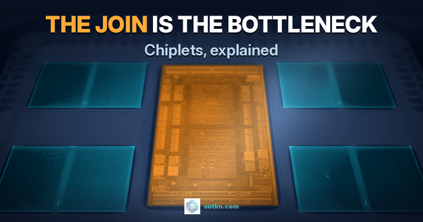
A lithography tool prints one field at a time. Low-NA's field is the reticle. Chiplet designs exist in part because that field has a hard size: Nvidia's Hopper GPU sat at 814 square millimetres, about 95% of one reticle (our arithmetic on Nvidia's Hot Chips 2024 figures). High-NA's field is half of that. A die that filled a Low-NA reticle does not fit one High-NA exposure. The foundry then has three choices, each with a cost: stitch two shots inside the die (two masks, a seam that has to yield — Intel's 6-inch PDK path); floor-plan into chiplets small enough for one shot, then join them on CoWoS or hybrid bonding; or wait for a 12-inch mask, which ASML and TSMC say removes stitching constraints, with a 2031 pilot and 2033 production systems.
None of those three is "High-NA replaces Low-NA this year." TSMC's N2 ramp still consumes Low-NA layers. ASML's 14 October release said supply as currently planned for 2027 and 2028 will not fully meet demand — that statement is footnoted to the July Low-NA and DUV capacity adds. High-NA is the insertion clock next to it. On 15 July Fouquet said High-NA still has to reach Low-NA maturity before it beats Low-NA-plus-immersion on cost. Q3's "availability approaching 90%" is progress on that sentence, not a plan of 65 EXE boxes.
Who gets paid — and where is the stuck step?
| Step | Who gets paid | Where cash sticks |
|---|---|---|
| Tool | ASML (optics with Zeiss) | One High-NA system recognised in Q2 inside €3.8B of EUV sales; one in Q3 inside €4.1B. Installed Base Management was €3.289B in Q3 — upgrades on the fleet already on the floor |
| Stuck step | Half-field stitch, or a die that does not fit | 6-inch masks need stitching or floor-planning. 12-inch masks, which remove that constraint, are a 2031–2033 clock |
| Foundry | Intel Foundry now on select 18A layers; TSMC from 2030 (plan); Samsung DRAM from 2028 (plan) | Paid when High-NA layers yield. Intel's select layers are dual-qualified to NXE, so Low-NA is still the backup |
| Neighbour gate | CoWoS-class packaging + HBM | A printed die still needs a stack and a slot. Who makes AI chips designs; TSMC and the OSATs join |
| Buyer | Hyperscalers and accelerator designers | Pay for modules, not for scanner backlog |
Cash sticks at ASML when an EXE is recognised and when the High-NA fleet is upgraded. Cash sticks at Intel Foundry when those select 18A layers ship. It sticks later at TSMC and Samsung if 2030 and 2028 hold. It still sticks at Low-NA for this year's ~65: Q3's EUV column was mostly NXE.
The US door is Intel's Oregon EXE line. Taiwan is TSMC's 2030 plan and the 12-inch mask. Korea is Samsung's 2028 DRAM High-NA plan, beside HBM. China does not buy EUV; who makes EUV machines is why that door stays closed.
A useful test, not a ticker call: if Q4 still recognises one High-NA system while Low-NA tracks ~65, insertion is not volume. If TSMC brings High-NA HVM forward from 2030, or 12-inch masks move earlier than 2031, the half-field bind eases. If stitching yield on 6-inch masks stays the tax on every reticle-class AI die, the join — not the press release — is still the stuck step.
What to check next
ASML Q4 2026: High-NA units against one system in Q2 and one in Q3, Low-NA against ~65. TSMC's next call: 2030 High-NA HVM and the 2031 12-inch pilot. Samsung: 2028 DRAM High-NA as a plan, not a shipment. Intel Foundry: whether 18A High-NA stays a dual-qualified subset. Layer: semiconductors.
Common misconceptions
- People assume High-NA has taken over from Low-NA. Actually Q3 2026 recognised one High-NA system inside €4.1 billion of EUV sales. The 2026 volume clock is still about 65 Low-NA systems, and 2027–2028 Low-NA supply is the one ASML says will not fully meet demand.
- People assume one million High-NA wafers means High-NA is printing every leading-edge die. Actually Intel and ASML count those wafers across certification, R&D, and volume production on select Panther Lake layers. The products are dual-qualified to Low-NA.
- People assume a High-NA scanner prints the same field as Low-NA, only sharper. Actually ASML's EXE:5000 needs an exposure field half the size of NXE. Dies that filled a Low-NA reticle must stitch, shrink, or wait on a 12-inch mask.
- People assume High-NA and CoWoS are the same bottleneck. Actually High-NA prints the die. CoWoS joins the die to HBM. A stitched layer that yields still waits on a packaging slot.
Not investment advice. Do your own research.
FAQ
What is High-NA EUV? High-NA EUV is the 0.55-numerical-aperture scanner that prints tighter layers than Low-NA EUV (0.33 NA) using the same 13.5-nanometre light. ASML's EXE family sells it. The EXE:5000 is specified at 8 nm resolution and a field half the size of NXE.
How is High-NA different from Low-NA EUV? Low-NA (NXE) is this year's volume clock — about 65 systems. High-NA (EXE) prints a tighter pitch on a half-size field. Q3 2026 recognised one High-NA system inside €4.1 billion of EUV sales. Stitching or floor-planning is required on today's 6-inch masks.
Why does High-NA print a smaller field? The 0.55 NA uses anamorphic mirrors that, ASML says, require an exposure field half the size of NXE systems. Intel Foundry and ASML call the join of two such shots half-field stitching.
Is High-NA replacing Low-NA this year? No. ASML still plans about 65 Low-NA systems in 2026, and says 2027 and 2028 Low-NA supply as currently planned will not fully meet demand. High-NA is insertion: one recognised system in Q2 and one in Q3.
Who gets paid when a High-NA scanner is recognised? ASML is paid on the EXE box and on Installed Base Management. Zeiss is paid on the optics. The foundry is paid when High-NA layers yield. Intel Foundry is the present volume user, on select 18A layers.
When will TSMC and Samsung use High-NA in volume? TSMC intends High-NA high-volume manufacturing for advanced nodes starting in 2030 (8 September 2026). Samsung plans High-NA on future DRAM high-volume manufacturing by 2028. Those are company plans, not this year's 65.
Does one million High-NA wafers mean High-NA is the volume clock? No. Intel Foundry and ASML count more than one million wafers across certification, R&D, and volume production on select Panther Lake layers, dual-qualified to Low-NA. That is insertion evidence, not a replacement for Low-NA output.
Related terms
EUV lithography · EUV vs DUV · Who makes EUV machines · Chiplet · CoWoS · Interposer · Hybrid bonding · Who makes AI chips
Markets and stack doors
Layer: Semiconductors. Company model: What does ASML do? · What does TSMC do?. Sibling layers: hyperscalers (who buy the modules) · neoclouds (who bill the hours after the module ships). Markets: Taiwan (TSMC 2030 High-NA and 12-inch masks) · Korea (Samsung 2028 DRAM High-NA) · US (Intel Oregon EXE line). Wire: ASML 2027–2028 supply.
How we check this
Figures come from company filings and company releases, dated below. The Q3 EUV versus High-NA split is the investor-call language; the 6-K prints the totals. The one-million-wafer count spans certification, R&D, and select layers. 2028 and 2030 HVM dates are plans, not shipments. Our arithmetic is shown in full.
Last reviewed: 21 Oct 2026 · Next review: after ASML Q4 2026 results print High-NA units against one system a quarter
Sources
- ASML — TWINSCAN EXE:5000 — 0.55 NA; 8 nm; 1.7× / 2.9× versus NXE; half-size field
- ASML — Q3 2026 results (14 Oct 2026) — €11,662m sales; IBM €3,289m; 113 new / 8 used systems; 2027–28 supply short of demand
- ASML — Q3 2026 financial results (14 Oct 2026) — Q4 guide €14.2–15.2bn; FY 2026 €44–45bn
- ASML — Q3 2026 investor call (14 Oct 2026) — €8.4bn systems, €4.1bn EUV including one High-NA; logic 54% / memory 46%; High-NA availability ~90%
- ASML — High-NA readiness milestone (15 Jul 2026) — Intel 18A select Core Ultra Series 3 layers; dual-qualified to NXE; EXE:5200B
- Intel Foundry and ASML (8 Sep 2026) — >1 million wafers across certification, R&D, and select production layers; 6-inch stitching
- ASML and TSMC — 12-inch masks (8 Sep 2026) — High-NA HVM from 2030; 12-inch pilot 2031; production systems 2033
- Samsung and ASML (8 Sep 2026) — DRAM High-NA HVM planned by 2028