
HBM vs DDR5
HBM stacks beside the GPU on advanced packaging; DDR5 sits as host memory on DIMMs. Same DRAM family tree — different stuck step and who gets paid. AI servers usually need both.
EXPLAINEDLast reviewed: 28 September 2026Next review: after next JEDEC HBM/DDR5 update or major HBM/DDR5 product ship note
HBM vs DDR5 is the contrast between high-bandwidth memory stacked beside an AI accelerator on advanced packaging and host/system DRAM on DIMMs off the package.
In short: HBM is stacked beside the GPU on advanced packaging. DDR5 is host DRAM on DIMMs. AI training and flagship inference pay the HBM + packaging path; the same server still buys DDR5 for system memory. Who gets paid and which step sticks are different — not a replacement contest.
For investors watching the semiconductors layer, the money link is simple: who gets paid when AI CapEx binds scarce HBM stacks and packaging, versus who gets paid when host DDR5 DIMMs ship for the same AI servers. This page is the contrast — not a tip sheet. AI racks usually need both memory classes.
What is the difference between HBM and DDR5?
HBM (high bandwidth memory) stacks DRAM dies vertically with through-silicon vias and sits beside the GPU on an interposer or advanced package. DDR5 (double data rate 5) is host/system DRAM on DIMMs in the CPU memory channels, off that package. That attach difference drives bandwidth density, packaging cost, power per bit, and which suppliers clear first when AI orders hit.
| Axis | HBM | DDR5 |
|---|---|---|
| Physical attach | Stacked DRAM on interposer / advanced package beside the GPU | DIMM modules in host memory channels off the package |
| Bus style | Very wide, package-level (e.g. 1024–2048-bit class per stack) | Two 32-bit channels per DIMM; board/CPU channel scaling |
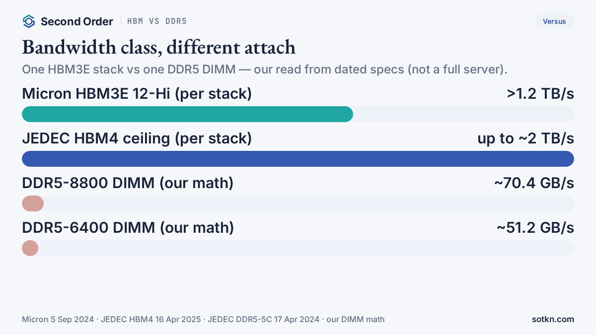
| Bandwidth class | ~1.2 TB/s per HBM3E stack (Micron, 5 Sep 2024); JEDEC HBM4 up to ~2 TB/s/stack (16 Apr 2025) | ~51.2 GB/s per DDR5-6400 DIMM; ~70.4 GB/s per DDR5-8800 DIMM (our JEDEC-style math) |
| Typical AI use | On-package memory for training and flagship inference GPUs (e.g. H200 141 GB HBM3e @ 4.8 TB/s) | Host/system memory for CPU, OS, orchestration, and capacity in the same AI server |
| Packaging tax | CoWoS / interposer / hybrid-bond economics | Standard DIMM / motherboard routing |
| Who gets paid | HBM suppliers + advanced packaging when CapEx binds stacks | DRAM / DIMM suppliers when host memory and capacity ship |
| Stuck step | Stack supply + packaging slots (short clock) | Usually wafer/module volume and platform speed — not the CoWoS gate |
Sibling contrast for graphics DRAM on the board: HBM vs GDDR. For the packaging gate next to HBM, see what CoWoS packaging is.
When does each win?
HBM wins when the workload saturates multi-TB/s on-package bandwidth and needs large capacity next to the die — training runs and flagship inference. NVIDIA’s H200 lists 141 GB of HBM3e at 4.8 TB/s (NVIDIA product page). Blackwell Ultra reaches 288 GB of HBM3E at 8 TB/s across eight 12-Hi stacks (NVIDIA Technical Blog).
DDR5 wins as host memory when the design needs capacity and channel bandwidth off the package — CPU-side working sets, OS, orchestration, and system buffers in the same AI server. JEDEC published JESD79-5C on 17 April 2024 with timing support up to 8800 Mbps. Micron’s 1 May 2024 AI data-centre note said it was first to validate and ship 128 GB DDR5 RDIMMs built on 32Gb dies while also supplying HBM3E for GPU-attached memory (company press).
Buyers usually need both tiers in one box. The useful question is which CapEx line is binding — scarce stacks and packaging, or host DIMM capacity and speed — not whether one acronym kills the other.
Who gets paid — and where money sticks?
On the HBM path, cash sticks when AI CapEx orders bind memory suppliers and advanced packaging. SK hynix began mass production of 12-layer HBM3E at 36 GB and 9.6 Gbps on 26 September 2024 (SK hynix Newsroom) — company-reported product claims, not guidance for every SKU. Micron’s HBM3E 12-high claims more than 1.2 TB/s at pin speeds above 9.2 Gb/s (Micron, 5 Sep 2024).
Our arithmetic from those dated ceilings: one Micron HBM3E stack at >1.2 TB/s versus one DDR5-6400 DIMM at 51.2 GB/s is about 23× (1200 ÷ 51.2 ≈ 23.4). Versus one DDR5-8800 DIMM at 70.4 GB/s it is about 17× (1200 ÷ 70.4 ≈ 17.0). JEDEC HBM4’s ~2 TB/s stack ceiling is about 28× one DDR5-8800 DIMM (2000 ÷ 70.4 ≈ 28.4). That is stack-versus-DIMM math — system bandwidth still depends on how many stacks the GPU wires versus how many host channels and DIMMs the platform populates.
| Step | HBM path | DDR5 path |
|---|---|---|
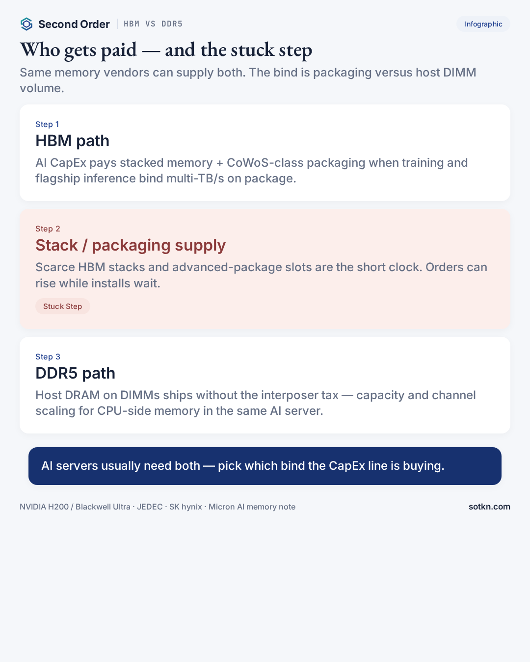
| Who gets paid first | Memory makers and packaging lines when AI accelerator BOM orders bind | DRAM and DIMM makers when host memory for AI servers ships |
| Where money sticks | Scarce HBM stacks and CoWoS-class finish lines with lag | Commodity DRAM / high-capacity RDIMM volume without the interposer tax |
| Stuck step | Orders vs installs — CapEx can rise while stacks and package slots wait | Rarely the same packaging bind; scales with platform channels and module supply |
Markets door for Korea memory allocation: Korea HBM — who gets paid when AI memory stays scarce. Analysis on where the stuck step moves next: If packaging catches up in 2027, where does the stuck step move?.
How does power and packaging compare?
HBM’s advantage is bandwidth density and energy per bit at the package when the workload saturates multi-TB/s. JEDEC HBM4 (16 Apr 2025) lists lower vendor-specific VDDQ options versus prior generations — a standard feature list, not a measured wattage for every part. DDR5’s advantage is host capacity and channel scaling with standard DIMM economics (JEDEC JESD79-5C, 17 Apr 2024). The packaging clock is the second-order read: HBM demand hits CoWoS-class slots; DDR5 host demand mostly does not.
For the tools that gate how fast HBM capacity can rise, see memory process tools for HBM.
Common misconceptions
- People assume HBM and DDR5 are interchangeable DRAM picks. Actually they share a DRAM family tree but diverge on attach, packaging tax, and which CapEx line clears first.
- People assume DDR5 replaces HBM on AI GPU BOMs. Actually flagship AI GPUs stay on HBM (NVIDIA H200 / Blackwell Ultra product specs). DDR5 remains host memory in the same server.
- People assume one big bandwidth number settles the debate. Actually compare stack versus DIMM carefully. System bandwidth is stacks × rate or channels × DIMMs × pin speed.
- People assume JEDEC ceilings equal shipping SKUs. Actually standards set envelopes. Vendor bins and GPU or server product pages are the shipping claims — labelled as company-reported.
FAQ
What is the difference between HBM and DDR5?
HBM is stacked DRAM on a silicon interposer or advanced package beside the GPU. DDR5 is host/system DRAM on DIMMs off the package. Bandwidth class, packaging cost, and who gets paid diverge from that attach.
Is HBM faster than DDR5?
Per stack versus one DIMM, yes in the AI class: Micron’s HBM3E 12-high claims more than 1.2 TB/s (5 Sep 2024), while one DDR5-6400 DIMM is about 51.2 GB/s and one DDR5-8800 DIMM about 70.4 GB/s from JEDEC-style channel math. System bandwidth still depends on stack count versus channel count and DIMM population.
Does DDR5 replace HBM on AI GPUs?
No. Flagship AI GPUs attach HBM on package (NVIDIA H200 lists 141 GB HBM3e at 4.8 TB/s). DDR5 remains host memory for the CPU and system. AI servers usually buy both memory classes.
Why do AI servers need both HBM and DDR5?
The GPU saturates multi-TB/s on-package HBM for model weights and activations. The host still needs capacity and bandwidth on DIMMs for the OS, orchestration, and CPU-side data paths. Micron’s 1 May 2024 AI data-centre memory note shipped both HBM3E and high-capacity DDR5 RDIMMs.
Who gets paid in the HBM path versus the DDR5 path?
On the HBM path, cash sticks at memory suppliers and advanced packaging when AI CapEx orders bind scarce stacks and CoWoS-class slots. On the DDR5 path, cash sticks at commodity DRAM and DIMM suppliers when host memory and capacity scaling ship.
What is HBM4 versus DDR5-8800 on paper?
JEDEC HBM4 (JESD270-4, 16 Apr 2025) targets up to about 2 TB/s per stack on a 2048-bit interface. JEDEC DDR5 JESD79-5C (17 Apr 2024) extends timing support up to 8800 Mbps — about 70.4 GB/s per DIMM from two 32-bit channels. Those are standard ceilings, not a single SKU guarantee.
Related terms
- HBM — high bandwidth memory stacked beside AI GPUs.
- HBM vs GDDR — stacked package memory versus planar graphics DRAM on the board.
- CoWoS — the packaging gate that often sits next to HBM.
- Memory process tools — equipment that gates how fast HBM capacity can rise.
Markets and stack doors
Layer: semiconductors. Markets: Korea HBM memory.
Further reading
Analysis: where the stuck step moves if packaging catches up.
Get the Wire — short notes when memory or packaging clocks move.
How we check this
Figures come from company filings and government releases, each dated in the list below. Capacity and timing from press reports are labelled as reported, not guided. Where we work something out ourselves, the arithmetic is shown in full.
Last reviewed: 28 Sep 2026 · Next review: after next JEDEC HBM/DDR5 update or major HBM/DDR5 product ship note
Spot an error? Tell us and we will correct it and note the change here.
Sources
- JEDEC — HBM4 (JESD270-4); up to ~2 TB/s on 2048-bit, up to 64 GB/stack (16 Apr 2025)
- JEDEC — DDR5 JESD79-5C; timing support up to 8800 Mbps (17 Apr 2024)
- Micron — HBM3E 12-high 36 GB; >1.2 TB/s at >9.2 Gb/s (5 Sep 2024)
- SK hynix — mass production of 12-layer HBM3E 36 GB at 9.6 Gbps (26 Sep 2024)
- NVIDIA H200 — 141 GB HBM3e at 4.8 TB/s (product page, accessed 28 Sep 2026)
- Micron / GlobeNewswire — ships 128 GB DDR5 RDIMMs for AI servers and supplies HBM3E (1 May 2024)
- NVIDIA Technical Blog — Blackwell Ultra: 288 GB HBM3E, 8 TB/s