What Is a Silicon Wafer? How It’s Made, Who Makes It, and Why Supply Is Tight
A silicon wafer is the blank disc every chip is built on. A small group of specialists makes them, much of it under multi-year contracts, and AI demand is now running into crystal-growing capacity that takes years to add.

EXPLAINED · Mechanism · Last reviewed: 13 Nov 2026 · Next review: after SEMI’s fourth-quarter 2026 wafer shipment count and the wafer makers’ fourth-quarter results
A silicon wafer is a thin, polished disc of single-crystal silicon, up to 300 mm across, on which chips are built.
In short. Every chip starts as a blank silicon wafer, bought from a small group of specialist makers. Wafer shipments rose 13.4% from a year earlier to 3,756 million square inches in the third quarter of 2026, led by AI logic and memory. Much of the volume is sold under multi-year agreements, some with prepayments, and the makers are now asking for higher prices on extra volume. Our read: the stuck step is the crystal itself. New crystal-pulling capacity takes years and must be qualified by each customer, and the makers say today’s prices do not yet pay for it.
Why an investor cares: every AI processor and every stack of HBM starts as a blank wafer bought from outside the fab. When those wafers get tight, the chipmaker’s plan waits, and the wafer maker gains pricing power it has not had for years. This page sits under our Semiconductors layer, upstream of everything else on it.
What is a silicon wafer?
A silicon wafer is the blank disc a chip is built on: a slice of one continuous silicon crystal, polished flat enough to print circuits measured in nanometres. A chipmaker, or fab, buys blank wafers, then deposits, prints and etches layer after layer of circuitry on them. At the end, the finished wafer is cut into individual chips.
The disc itself carries no circuits. Its job is to be perfect: one crystal with its atoms in a regular lattice, almost no impurities, and a surface flat and clean to within atoms. Any defect in the wafer becomes a defect in the chips printed on it.
SEMI, the industry association, describes wafers as the substrate on which most semiconductors are made, in diameters of up to 300 mm. What gets built on top is covered in our 2nm chip Explained; how many of those chips survive is in our semiconductor yield Explained.
| Wafer type | What it is | Main uses |
|---|---|---|
| Polished | Sliced from the ingot, then lapped, etched and mirror-polished | Memory (DRAM, HBM, NAND), many mature chips; bonding and packaging carriers |
| Epitaxial (epi) | Polished wafer with a thin, very pure crystal layer grown on top | Leading-edge logic such as AI processors; power chips |
| Silicon-on-insulator (SOI) | Thin silicon layer on an insulating oxide layer | RF chips, power devices, silicon photonics |
| Test and monitor | Wafers used to check tools and processes, not sold as chips | Fab set-up and process control |
Second Order summary of SEMI and company product descriptions.
How is a silicon wafer made?
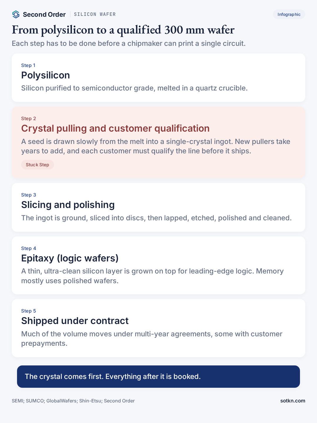
A silicon wafer is made by growing a single crystal, slicing it and polishing the slices. The steps run in a fixed order, and each one has its own specialist equipment.
- 1. Purify. Polysilicon is refined to semiconductor grade, far purer than the material used in solar panels.
- 2. Pull the crystal. The polysilicon is melted in a quartz crucible. A small seed crystal is dipped in and drawn slowly upward while it turns, so the melt freezes onto it as one crystal. This is the Czochralski method. The result is a cylindrical ingot, rounded at the seed end like the one in the photo above.
- 3. Shape and slice. The ingot is ground to an exact diameter and sliced into thin discs with wire saws.
- 4. Lap, etch and polish. The discs are flattened, chemically etched to remove damage, and polished to a mirror finish.
- 5. Grow an epitaxial layer, if needed. For leading-edge logic, a thin layer of extra-pure crystal is grown on the polished surface.
- 6. Clean, inspect and ship. Each wafer is cleaned, measured and sealed in a pod for the fab.
- 7. Qualify. Before a new line or plant can supply a chipmaker, the customer tests its wafers in its own process. GlobalWafers says its new Texas plant is ramping as customer qualifications advance.
The fab that receives the wafer is a different business, with its own clean rooms and tool makers. The wafer maker’s work ends where the fab’s begins.
What sizes do silicon wafers come in?
Silicon wafers come mainly in 300 mm and 200 mm diameters, with smaller sizes for older devices. A 300 mm wafer has about 109.6 square inches of area, 2.25 times a 200 mm wafer, by our arithmetic. More area per wafer means more chips per pass through the fab, which is why every leading-edge plant is built for 300 mm.
| Diameter | Area | Where it is used |
|---|---|---|
| 300 mm (12-inch) | About 109.6 sq in | Leading-edge logic, DRAM and HBM, NAND, and a growing share of power and specialty chips |
| 200 mm (8-inch) | About 48.7 sq in | Power devices, analog, sensors, automotive and industrial chips |
| 150 mm and smaller | 17.4 sq in or less | Discrete and legacy devices |
Areas are Second Order arithmetic from the diameter. Uses from SEMI, SUMCO and Shin-Etsu commentary.
The two sizes serve different markets, and in 2026 both are tightening for different reasons. SUMCO said 300 mm demand was being driven by advanced logic and memory for AI and data centres, while 200 mm demand was rising for AI-related power devices.
How many silicon wafers does the world use?
The world shipped 3,756 million square inches of silicon wafers in the third quarter of 2026, according to SEMI. That was 13.4% more than a year earlier and 5.1% more than the second quarter. The industry counts by area, not by wafers, so that different diameters can be added together.
If all of that area were 300 mm wafers, it would be about 34.3 million wafers in the quarter, or about 11.4 million a month, by our arithmetic. The real count is higher, because part of the area is in smaller wafers.
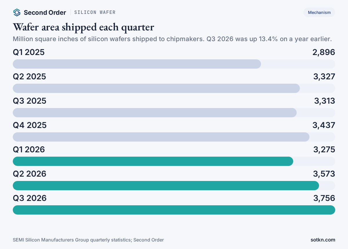
The first nine months of 2026 added up to 10,604 million square inches, 11.2% more than the same months of 2025, by our arithmetic. SEMI’s annual forecast, published on 21 October 2026, expects 14,420 million square inches for the full year, up 11.8%, and successive records to 17,034 in 2029. That is about 18% more over three years, or roughly 5.7% a year, by our arithmetic.
Shin-Etsu gave the same picture from inside the market. On 27 October 2026 it said the wafer market rose by a mid-single-digit percentage in the July to September quarter and by just over 10% on a year earlier, with 300 mm wafers following the same pattern.
Why does AI use more silicon wafers?
AI uses more silicon wafers because it needs more chips of every kind, and many of those chips use more silicon per unit of output. SEMI and the wafer makers point to five sources of demand.
- Leading-edge logic. AI processors are built on epitaxial 300 mm wafers. SUMCO said chiplet designs for GPUs and CPUs are lifting logic wafer demand across several process generations, not only the newest.
- Memory, beyond HBM. SEMI’s forecast says memory demand extends from HBM to server DRAM and enterprise NAND, all on polished 300 mm wafers. Our HBM Explained covers why each stack needs so much silicon.
- Bonding and advanced packaging. SEMI said bonding and packaging continued to support demand for 300 mm polished wafers. Silicon is used as carrier wafers and as the interposer under an AI chip, and hybrid bonding stacks wafers on wafers.
- Photonics. GlobalWafers said its output of 12-inch silicon-on-insulator wafers hit a record, with demand for silicon photonics, RF and power uses above its expansion plan. Our silicon photonics Explained covers the optical side.
- Power devices. SEMI said AI demand had broadened to power devices and that AI server power supplies were lifting industrial demand. Siltronic said demand for 200 mm wafers was increasingly strong.
Who makes silicon wafers?
Silicon wafers are made by a small group of specialist companies, not by the chipmakers themselves. The best known are Shin-Etsu Chemical and SUMCO in Japan, GlobalWafers in Taiwan, Siltronic in Germany and SK Siltron in South Korea. Four of them reported results in the past three weeks.
| Maker | Home | Latest quarter (reported) | What it said about supply |
|---|---|---|---|
| Shin-Etsu Chemical | Japan | July–Sept 2026 (27 Oct) | Customers opening talks on next contracts early; higher prices asked for extra volume; only limited brownfield additions in the first half of next year |
| SUMCO | Japan | July–Sept 2026 (11 Nov) | Sales ¥117.5bn; contract prices held; 300 mm demand outrunning requested volumes; new capacity not economic at current prices |
| GlobalWafers | Taiwan | July–Sept 2026 (3 Nov) | Revenue NT$14.87bn; all diameters at full utilisation; NT$21.2bn of customer prepayments; 10-year deal with Micron |
| Siltronic | Germany | July–Sept 2026 (4 Nov) | Sales €355.4m, up 10.5% on volume; prices barely moved; new 300 mm capacity in Singapore |
| SK Siltron | South Korea | Not listed separately | Part of SK Group; not covered by the sources on this page |
From each company’s results materials listed under References. Not a ranking.
The group is tied together in places. GlobalWafers holds shares in Siltronic, and its own results swing with their market value. Siltronic’s newest 300 mm capacity is in Singapore, and the company said that expansion is how it is supporting AI-driven growth. GlobalWafers has a new plant in Texas, a 12-inch silicon-on-insulator plant in Missouri, a new 12-inch line in Novara, Italy, and plants in Japan.
Their customers are the foundries and memory makers. Our who makes HBM page covers the memory side of that customer list.
How are silicon wafers sold?
Much of the world’s silicon wafer volume is sold under long-term agreements: multi-year contracts that set volumes and prices, sometimes backed by a customer prepayment. The rest is sold on shorter terms, and that is where prices move first.
- Contract prices held. SUMCO said long-term agreement prices were maintained in the third quarter of 2026, and that it would serve extra demand based on existing customer relationships and prices.
- Extra volume costs more. Shin-Etsu said it had asked customers to accept higher prices for additional volumes, and that for some customers increases would apply from October 2026. It is also negotiating with customers that have no long-term agreement.
- Next contracts are opening early. Shin-Etsu said more customers had begun negotiating their next contracts while existing ones were still in force, out of concern about further supply limits.
- Customers pay ahead. GlobalWafers reported NT$21.2 billion of customer prepayments, about US$0.67 billion, or roughly 1.4 times its third-quarter revenue, by our arithmetic. Micron agreed to subscribe to up to US$500 million of a 10-year GlobalWafers convertible bond, alongside a planned 10-year supply agreement.
The logic is the same as a purchase commitment on the buyer’s side: the customer locks in supply for years, and in return the supplier gets visibility and, sometimes, cash up front to build.
Who gets paid?
Our read: the wafer makers are paid first, the customers who signed long contracts are protected, and the buyers without contracts pay the new price.
- Wafer makers, on volume first. Siltronic’s third-quarter sales rose 10.5% on the quarter to €355.4 million, driven by higher wafer area sold; it said price and product mix had only a limited effect. SUMCO’s 300 mm shipments rose sharply. The money so far comes from volume. Price is the next step, starting with extra volume and new contracts.
- Not yet on margin. The makers are still carrying the cost of the last build-out. SUMCO earned an operating profit of ¥2.0 billion on ¥117.5 billion of sales in the third quarter, a 1.7% margin, while its EBITDA margin was 29.8%: depreciation took about 94% of EBITDA, by our arithmetic. Siltronic’s gross profit was −€7.5 million, with about a third of its cost of sales in depreciation.
- Chipmakers with long contracts. They pay the agreed price and get first claim on volume. Shin-Etsu said leading-edge logic wafers are priced more finely by specification, so a richer mix lifts its average price even before any increase.
- Buyers without contracts. They face the price increases first and are served after contract customers.
- Customers funding supply. Micron’s bond and GlobalWafers’ prepayments show the customer paying part of the cost of new capacity in exchange for a place in the queue. Our Analysis on memory sold years ahead follows the same pattern one step downstream.
Where is the stuck step?
Our read: the crystal itself. Wafer demand can rise in a quarter, but new crystal-pulling and polishing capacity takes years to build and then has to be qualified by each customer. Until it is, the only extra supply is what existing lines can squeeze out.
The makers say so in their own words. SUMCO said on 11 November 2026 that 300 mm supply was becoming unable to meet the volumes customers request in the fourth quarter. It added that, at current prices and with costs rising, adding capacity is not economically rational, and would take several years even if it were decided, so supply and demand would tighten further.
Shin-Etsu said it would be able to raise output only to a limited extent in the first half of next year, through brownfield expansion at existing sites, and that greenfield costs have risen considerably. GlobalWafers said high construction costs, long equipment lead times and qualification cycles limit how fast new supply can be added, and that its capacity across all diameters is fully used.
The spending numbers show the same caution. SUMCO spent ¥29.7 billion on capital projects in the first nine months of 2026 against ¥99.2 billion of depreciation, about 30%, by our arithmetic. Siltronic expects capital spending of €180 million to €200 million in 2026 against €480 million to €500 million of depreciation. Both are running well below their depreciation.
Our photomask Explained covers another upstream input with the same shape: few suppliers, long qualification, and no quick fix when demand jumps.
What would change the view?
- Prices move on contracts, not just extra volume. If new long-term agreements reset at higher prices, the makers would have a reason to build, and the stuck step would start to ease in a few years.
- Capacity is announced. A greenfield 300 mm crystal-pulling plant from any major maker would signal that prices now cover the cost. SUMCO and Shin-Etsu both said they were not there yet.
- Demand pauses. Shin-Etsu expects volume to be roughly flat in the October to December quarter, partly because of maintenance shutdowns. A second flat quarter without maintenance would point to softer demand, not tight supply.
- Supply shocks. GlobalWafers’ third-quarter revenue slipped 2.3% on the quarter after a fire on the 8-inch line at its Italian plant, which shows how one site can move a quarter. Another outage would tighten things faster.
The clocks: Shin-Etsu’s price increases for some customers apply from October 2026; its limited brownfield additions arrive in the first half of 2027; contracts running into 2028 and beyond are being negotiated now; and SEMI’s fourth-quarter 2026 count and the makers’ fourth-quarter results will show whether prices, not just volumes, have started to move.
Common misconceptions
- People assume chipmakers make their own wafers. Actually they buy blank wafers from specialist makers such as Shin-Etsu, SUMCO, GlobalWafers, Siltronic and SK Siltron, then build circuits on them.
- People assume “wafers” in fab news are the same thing. Actually fab wafer starts count blank wafers entering a production line. Wafer makers sell the blanks, and the industry measures them by area.
- People assume rising shipments mean rising profits. Actually depreciation from the last build-out still absorbs most of the gain. SUMCO’s third-quarter operating margin was 1.7%.
- People assume more demand quickly brings more supply. Actually new capacity takes years and needs customer qualification, and SUMCO says today’s prices do not yet justify building it.
FAQ
What is a silicon wafer?
A silicon wafer is a thin, polished disc of single-crystal silicon, up to 300 mm across, on which chips are built. Chipmakers buy blank wafers and print, etch and deposit circuits on them; how many chips fit on one wafer depends on the size of each chip.
What is a silicon wafer used for?
Silicon wafers are the starting material for most semiconductors: processors, memory, power chips, sensors and photonics. They are also used as test wafers in fabs and, increasingly, as carrier and bonding wafers in advanced packaging.
How is a silicon wafer made?
Purified polysilicon is melted and a single crystal is pulled slowly from the melt to form an ingot. The ingot is ground, sliced into thin discs, then lapped, etched, polished and cleaned. Some wafers get an extra epitaxial layer of silicon grown on top before inspection and shipment.
Who makes silicon wafers?
A small group of specialist companies makes them. The best known are Shin-Etsu Chemical and SUMCO in Japan, GlobalWafers in Taiwan, Siltronic in Germany and SK Siltron in South Korea. Chipmakers such as foundries and memory makers are their customers; Micron, for example, has agreed to fund GlobalWafers through a 10-year bond.
Why are 300 mm wafers so important for AI?
Leading-edge logic and memory, including AI processors and HBM, are made almost entirely on 300 mm wafers. SEMI’s 2026 forecast says AI demand is supporting epitaxial wafers for leading-edge logic and polished wafers for memory, and SUMCO says 300 mm demand is outrunning the volumes customers request.
How are silicon wafers measured?
The industry counts wafers by area, in millions of square inches (MSI), so different diameters can be added together. A 300 mm wafer has about 109.6 square inches of area, 2.25 times a 200 mm wafer, by our arithmetic.
Why don’t wafer makers just build more capacity?
Because a new crystal-growing and polishing line costs a lot, takes years, and must be qualified by each customer before it can ship. SUMCO said on 11 November 2026 that adding capacity is not economically rational at today’s prices and would take several years even if approved.
Is this a list of stocks to buy or sell?
No. This page explains how silicon wafers are made, sold and paid for. It does not rank companies or give buy or sell calls. Not investment advice. Do your own research.
Related: semiconductor yield; photomask; clean room; interposer; hybrid bonding; who makes wafer fab equipment.
Stack doors
Layer: Semiconductors. Markets: Taiwan and Korea. Markets note: Micron’s Idaho build in its annual report.
Get the Wire — short daily notes on where AI computing gets built and who pays for it.
Not investment advice. Do your own research.
How we check this
Quarterly wafer shipments and the 2026–2029 forecast come from SEMI’s Silicon Manufacturers Group releases of 4 November and 21 October 2026 and its published quarterly statistics. Shin-Etsu’s market comments, contract talks, pricing and capacity plans come from its first-half results call summary of 27 October 2026. SUMCO’s results, contract prices, demand outlook and capacity view come from its third-quarter presentation and earnings summary of 11 November 2026. GlobalWafers’ results, plant updates, prepayments and the Micron agreement come from its results release and earnings call presentation of 3 November 2026. Siltronic’s results, pricing comment, depreciation and Singapore expansion come from its release of 4 November 2026. Company statements about demand and capacity are their own outlooks, not facts about the future. Wafer areas, 300 mm equivalents, margins, growth rates and ratios are our arithmetic, checked in code and labelled as ours on the page. SEMI’s quarterly series includes non-polished wafers and its annual forecast does not, so we do not add the two together. Who gets paid and the stuck step are our read. The featured photograph is credited in its caption. This page explains a material and how it is sold. It does not rank companies or give buy or sell calls. Not investment advice. Do your own research.
Last reviewed: 13 Nov 2026 · Next review: after SEMI’s fourth-quarter 2026 wafer shipment count and the wafer makers’ fourth-quarter results
Spot an error? Tell us and we will correct it and note the change here.
References
- SEMI — Worldwide silicon wafer shipments increase 13.4% year-on-year in Q3 2026 (4 Nov 2026), with SEMI quarterly silicon shipment statistics — 3,756 million square inches shipped in Q3 2026, up from 3,313 a year earlier and 3,573 in Q2; AI demand broadening to power devices and photonics; 300 mm polished wafers for bonding and advanced packaging; quarterly series from 2025
- SEMI — SEMI forecasts 11.8% growth in silicon wafer shipments in 2026, with record highs expected through 2029 (21 Oct 2026) — 14,420 million square inches forecast for 2026 and 17,034 for 2029; epitaxial wafers for leading-edge logic and polished wafers for memory, including HBM, server DRAM and enterprise NAND
- Shin-Etsu Chemical — Summary of telephone conference on financial results for the first half ended 30 Sep 2026 (27 Oct 2026) — Wafer market up mid-single digits quarter on quarter and just over 10% year on year; customers opening talks on next long-term agreements early; higher prices for extra volumes, from October for some customers; limited brownfield additions in the first half of next year
- SUMCO Corporation — Third-quarter 2026 results presentation (11 Nov 2026), with the third-quarter earnings summary (kessan tanshin) filed the same day — Q3 sales ¥117.5 billion and operating profit ¥2.0 billion; long-term agreement prices held; 300 mm demand outrunning requested volumes in Q4; new capacity not economically rational at current prices and would take several years; nine-month capital spending and depreciation
- GlobalWafers — GlobalWafers reports Q3 2026 results (3 Nov 2026) — Q3 revenue NT$14.87 billion, gross margin 20.0%; Texas shipments at records with demand above capacity as customer qualifications advance; Missouri 12-inch SOI output at a record; Novara 8-inch fire
- GlobalWafers — Q3 2026 earnings call presentation (3 Nov 2026) — Customer prepayments of NT$21.2 billion (US$0.67 billion); up to US$500 million 10-year convertible bond with Micron as the only subscriber, alongside a planned 10-year long-term agreement; capacity at full utilisation across all diameters
- Siltronic AG — Siltronic slightly raises sales guidance for 2026 (4 Nov 2026) — Q3 sales €355.4 million, up 10.5% on Q2, from higher wafer area sold; price and mix had limited impact; gross profit −€7.5 million with about one-third of cost of sales in depreciation; 300 mm expansion in Singapore