
Explained
Who Makes HBM
Who makes HBM is the map of roles along the stack — memory makers, package attach, and tools. Allocation locks are not settled cash. Roles only. No tip sheet.
Writes Second Order by TKN — a plain-English map of AI infrastructure and semiconductors for non-specialist investors. Focus: who gets paid, where money sticks, and which step is stuck. Not investment advice.
Explained
Who makes HBM is the map of roles along the stack — memory makers, package attach, and tools. Allocation locks are not settled cash. Roles only. No tip sheet.
Wire
TrendForce keeps CoWoS-L as the mainstream AI packaging path through 2028. Packaging, not wafer starts, still sets the short clock.
Analysis
Hanmi Semiconductor sits at the memory stuck step with the bonders every HBM stack needs. At roughly ₩22 trillion, the question is what growth and margin that price already assumes.
China
September 2026 in one line: Beijing’s computing-network meeting makes power–computing coordination the gate — green-power direct connection, source-grid-load-storage, planning link — while NEA clocks computing electricity at +>100 TWh/yr toward ~800 TWh by 2030.
Explained
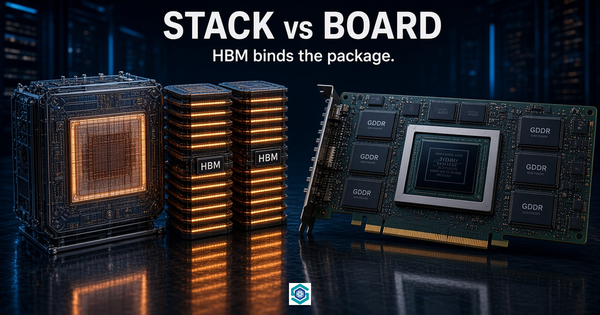
HBM stacks beside the GPU on advanced packaging; GDDR sits as discrete chips on the board. Same memory family tree — different stuck step and who gets paid.
Analysis
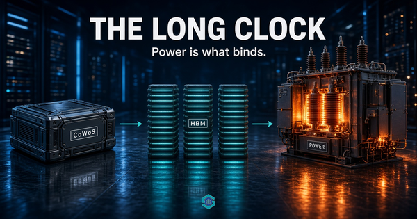
Advanced packaging has been the step the whole AI build chain waits for since 2024. Reported capacity plans put that gap closing through 2027. This piece works out what binds next — and it is not the step most people assume.
Wire
Nebius raises on-demand GPU prices up to 21% from 1 October. The spread is widening; capacity is arriving and prices are still going up.
US
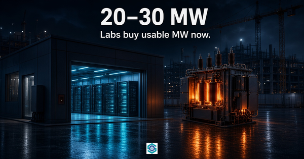
September 2026 in one line: Anthropic and OpenAI are sounding out 20–30 MW capacity deals to get usable compute faster than gigawatt campuses allow — while still holding multi-hundred-MW and GW commitments.
Korea
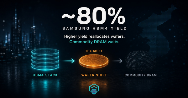
September 2026 in one line: Samsung’s HBM4 yield is near 80%, HBM wafer starts are headed toward ~250k a month, and commodity DRAM plus external foundry buyers compete for what’s left of wafer and SF4 capacity.
Explained
A neocloud is a specialist cloud that bills GPU clusters for AI work. What it is, how it earns, and why utilisation and realised price decide everything.
Explained
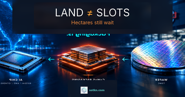
CoWoS is chip-on-wafer-on-substrate — TSMC’s packaging family that joins a compute die and HBM. How variants differ, and why hectares on a form are not packaging slots.
Explained
A neocloud bills accelerator time; a hyperscaler sells a broad cloud with GPUs as one line. Compare funding, pricing, lock-in, and what a demand dip hits.