What Is a TPU? Google’s Tensor Processing Unit, Explained
A TPU, or tensor processing unit, is a chip Google designs for one job: the large matrix math that trains and runs AI models. Broadcom builds and ships it. Google earns only once the chip runs in a powered, finished hall.
EXPLAINED · Mechanism · Last reviewed: 07 Oct 2026 · Next review: after Alphabet Q3 2026 results (28 Oct 2026)
A TPU, or tensor processing unit, is a chip Google designs for one job: the large matrix math that trains and runs AI models. Google Cloud calls it a custom application-specific integrated circuit, or ASIC.
In short. A TPU sits on the Semiconductors layer. Google designs it. Broadcom turns the design into a chip and ships it. Each Ironwood TPU carries 192 GiB of high-bandwidth memory. Broadcom is paid when the chip ships. Google earns, and the lab gets the compute it pays for, only once the chip runs in a powered, finished hall. That gap is the stuck step. Broadcom’s AI chip revenue was $16.7 billion in its quarter to 2 August 2026.
Why an investor cares: TPU money now shows up in several companies’ results, at different times. Broadcom books it when chips ship. Google books it when hours are used or systems are delivered. A lab like Anthropic pays over years. Knowing which step comes first tells you whose numbers move first. For the wider map of chip roles, see who makes AI chips.
What is a TPU?
A TPU is a chip built for matrix math. Training and running an AI model is mostly multiplying large grids of numbers. A TPU does that one job. It is an ASIC, an application-specific chip, rather than a chip built for every kind of work.
Google’s documentation says TPUs train models using hardware designed for “large matrix operations often found in machine learning algorithms.” They have high-bandwidth memory on the chip package, and they link together in groups called slices.
How does a TPU work?
Three parts do the work: matrix units, memory and links.
The matrix unit, or MXU, is the core. Google Cloud describes it as a 128 by 128 systolic array. That is a grid of small multipliers that pass results to their neighbours, so numbers flow through the grid instead of going back to memory each step.
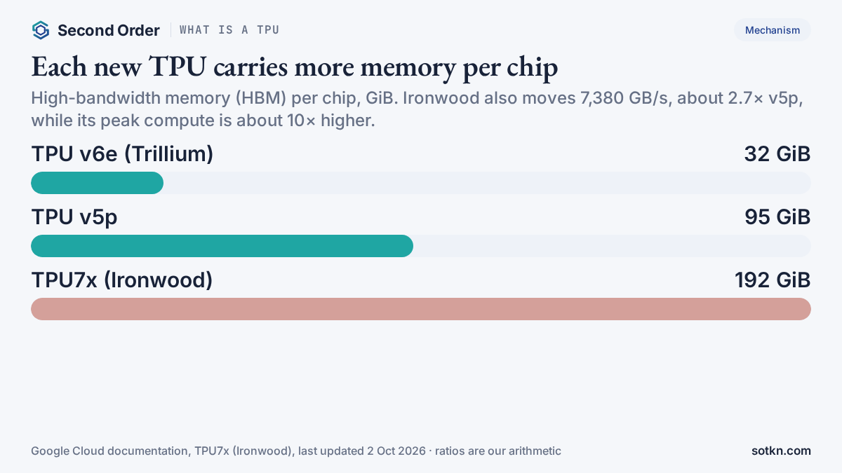
Memory feeds the grid. Each Ironwood chip has 192 GiB of HBM, moving 7,380 GB/s. For how that memory is built, see HBM, explained. For how it sits next to the chip, see CoWoS, explained.
Links join the chips. Ironwood chips connect in a 3D torus, and a single pod scales to 9,216 chips. A full pod holds about 1.77 million GiB of HBM (9,216 × 192 GiB = 1,769,472 GiB, our arithmetic).
| Google Cloud TPU | TPU7x (Ironwood) | v5p | v6e (Trillium) |
|---|---|---|---|
| Chips per pod | 9,216 | 8,960 | 256 |
| Peak compute per chip, FP8 (TFLOPs) | 4,614 | 459 | 918 |
| HBM per chip (GiB) | 192 | 95 | 32 |
| HBM bandwidth per chip (GB/s) | 7,380 | 2,765 | 1,638 |
| TensorCores per chip | 2 | 2 | 1 |
Source: Google Cloud documentation, TPU7x (Ironwood), last updated 2 Oct 2026.
Ironwood is the seventh generation. Against v5p, it has about 2.0 times the memory per chip, 2.7 times the memory bandwidth and 10 times the peak FP8 compute (192 ÷ 95; 7,380 ÷ 2,765; 4,614 ÷ 459, our arithmetic). Compute grew faster than memory. Google’s own docs warn that “HBM can still be a bottleneck” for memory-bound work.
TPU vs GPU: what is the difference?
A GPU is a general-purpose parallel chip. A TPU is Google’s own chip, built for matrix math. Both put HBM next to the compute. Google Cloud’s own guide sets out which work fits which.
| TPU | GPU | |
|---|---|---|
| What it is | An ASIC: built for the matrix math in AI | A general-purpose parallel chip, used for AI and much else |
| Who designs it | Google; Broadcom develops and supplies the chip | Chip companies such as Nvidia and AMD |
| How you get it | Pay by the hour on Google Cloud; since Q2 2026, TPU systems delivered into your own data centre | Buy servers, or pay by the hour at a cloud or neocloud |
| Best fit, per Google Cloud | Models dominated by matrix math, large batches, training for weeks or months | Models with many custom operations that must run partly on CPUs |
| Memory | HBM on the package: 192 GiB per Ironwood chip | HBM on the package too |
Who makes Google’s TPU?
Google designs it. Broadcom builds it. Broadcom’s Form 8-K of 6 April 2026 says it has a Long Term Agreement to develop and supply custom TPUs for Google’s future generations. A second agreement covers networking and other parts for Google’s next AI racks through up to 2031.
On its 2 September 2026 call, Broadcom said it delivered Ironwood “in high volume to both Anthropic and Google” in the quarter. It also began production shipments of the next generation, TPU v8i, for Google, which it said has more memory and bandwidth than Ironwood.
The chip needs three scarce inputs. Broadcom named them on the same call: leading-edge wafers, substrates and HBM memory. Each one, it said, can become the bottleneck at different times.
Who gets paid when a TPU is built?
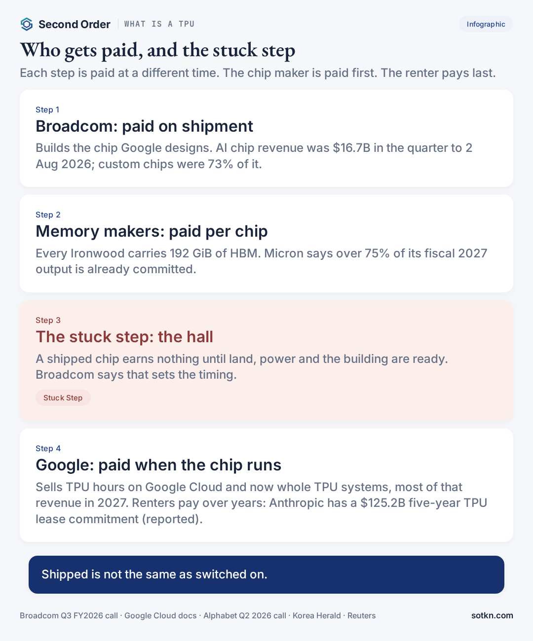
Broadcom is paid when the chip ships. Its AI semiconductor revenue was $16.7 billion in the quarter to 2 August 2026, up 221% on a year earlier. Custom accelerators, which it calls XPUs, were 73% of that, about $12.2 billion (0.73 × $16.7 billion, our arithmetic). That pool covers all six of its XPU customers, not only TPUs. It guides $21.7 billion of AI revenue for the next quarter.
Memory makers are paid for the HBM on every chip. Broadcom said rising memory content in its XPUs is pulling its consolidated gross margin down, to a guided 73% in Q4. Micron said more than 75% of its fiscal 2027 output is already committed, the Korea Herald reported on 1 October 2026. See who makes HBM and Micron’s 2027 commitments.
Google is paid two ways. It sells TPU hours on Google Cloud, which grew revenue 82% to $24.8 billion in Q2 2026. And it now sells whole TPU systems. Alphabet said it delivered TPU systems to customer data centres for the first time in Q2. It expects a “relatively small portion” of that revenue this year and the “vast majority” in 2027. Google also pays first: its capex was $44.9 billion in Q2, mostly on technical infrastructure, about 60% of that on servers. See what a hyperscaler is.
The lab pays to use them. Anthropic said in October 2025 it plans to use up to one million TPUs, worth tens of billions of dollars, with well over a gigawatt online in 2026. Its IPO prospectus shows a $125.2 billion five-year TPU lease commitment, Reuters reported on 1 October 2026. Broadcom agreed to lend up to $42 billion, about a third of it (42 ÷ 125.2 = 33.5%, our arithmetic). See Broadcom’s chip financing and who finances AI chip clusters.
Where is the stuck step for TPUs?
The hall. A TPU can be made, shipped and billed by Broadcom before it does any paid work. It earns for Google and the lab only once it is racked, powered and cooled in a finished building.
Broadcom said so on 2 September 2026. Its chief executive said land, power and shell “dictates specific timing of when this capacity gets deployed.” Of his own outlook, he asked: “even as we ship the chips, are they going to be deployed on a timely basis?”
Alphabet shows the same gap from the other side. It said it is “supply constrained,” will use third-party capacity in Q3 as a bridge, and expects most TPU-system revenue in 2027, not 2026.
Memory is the second pinch. It sits on the chip itself. Each new TPU carries more HBM, and memory makers have already committed most of next year’s output. For why memory binds briefly and power binds for years, see where the stuck step moves next.
Contracts carry the gap. Broadcom’s 8-K says Anthropic’s use of the extra capacity “is dependent on Anthropic’s continued commercial success.” Anthropic’s prospectus warns that some defaults could make a large part of its lease payments due at once, Reuters reported.
How big is the TPU build?
Big, and measured in gigawatts. Broadcom said on 2 September that, after 1 GW of Ironwood for Anthropic in 2026, it expects Anthropic to deploy another 5 GW of TPU v8i in 2027. Its April 8-K put Anthropic’s access through Broadcom at about 3.5 GW from 2027. The later figure is an expectation on a call, not a filed agreement.
For Google itself, Broadcom said it plans to deliver “multi-tens of billions of dollars of TPUs annually over the next several years.” It sees AI chip revenue of about $115 billion in fiscal 2027 and $230 billion in fiscal 2028, and says it has secured the supply for both. It put its own content at $20 billion to $30 billion per gigawatt.
| Date | What happened or is due | Source |
|---|---|---|
| 23 Oct 2025 | Anthropic plans up to one million TPUs; well over 1 GW online in 2026 | Anthropic |
| 6 Apr 2026 | Broadcom–Google deal to develop and supply future TPUs; Anthropic ~3.5 GW via Broadcom from 2027 | Broadcom 8-K |
| Q2 2026 | First TPU systems delivered to customer data centres | Alphabet call, 22 Jul 2026 |
| Quarter to 2 Aug 2026 | Ironwood shipped in high volume; TPU v8i production shipments begin | Broadcom call, 2 Sep 2026 |
| 1 Oct 2026 | $125.2B five-year TPU lease commitment; up to $42B Broadcom financing | Anthropic prospectus, as reported by Reuters |
| 28 Oct 2026 | Next check: Alphabet Q3 2026 results | Alphabet |
| 9 Dec 2026 | Next check: Broadcom Q4 FY2026 results | Broadcom |
| 2027 | Most TPU-system revenue expected; Anthropic’s ~3.5 GW via Broadcom begins | Alphabet; Broadcom 8-K |
What to check next
Three dated checks. 28 October 2026 (US time): Alphabet’s Q3 results, for TPU-system revenue and capex against its $195–205 billion 2026 guide. 9 December 2026: Broadcom’s Q4 results, against its $21.7 billion AI revenue guide. Through 2027: whether Anthropic’s 3.5 GW via Broadcom starts on time. That is the real test of whether the halls keep up with the chips.
Common misconceptions
- People assume a TPU is just Google’s GPU. Actually it is an ASIC built for matrix math. Google’s own guide sends models with many custom operations to GPUs.
- People assume only Google uses TPUs. Actually Anthropic plans up to one million, and Alphabet began delivering TPU systems to customer data centres in Q2 2026.
- People assume Google makes TPUs alone. Actually Broadcom develops and supplies them, under a long-term agreement filed on 6 April 2026.
- People assume a shipped chip is earning. Actually it earns only once the hall is powered. Alphabet expects most TPU-system revenue in 2027.
FAQ
What is a TPU?
A TPU, or tensor processing unit, is a chip Google designs for the large matrix math that trains and runs AI models. Google Cloud calls it a custom application-specific integrated circuit, or ASIC. It is built for one kind of work, not for everything.
What does TPU stand for?
TPU stands for tensor processing unit. A tensor is a grid of numbers, the form an AI model’s data and weights take. The chip is built to multiply those grids quickly.
What is Google’s latest TPU?
Ironwood, also called TPU7x, is the seventh generation and the newest with full specs in Google Cloud’s documentation. Each chip has 192 GiB of HBM and 4,614 peak FP8 TFLOPs. Alphabet also lists TPU 8t and 8i, and Broadcom began production shipments of TPU v8i for Google in its quarter to 2 August 2026.
Is a TPU better than a GPU?
It depends on the work. Google Cloud’s own guide points models dominated by matrix math, with large batches, that train for weeks or months, to TPUs. It points models with many custom operations that must run partly on CPUs to GPUs.
Can you buy a Google TPU?
Mostly you pay for one by the hour, on Google Cloud. Since the second quarter of 2026 Google also sells whole TPU systems, delivered into customers’ own data centres. Alphabet expects the vast majority of that revenue in 2027.
Who makes Google’s TPU chips?
Google designs them and Broadcom develops and supplies them. Broadcom’s 8-K of 6 April 2026 describes a Long Term Agreement to develop and supply custom TPUs for Google’s future generations.
How does Google make money from TPUs?
Two ways. It sells TPU hours through Google Cloud, whose revenue rose 82% to $24.8 billion in Q2 2026. And it sells TPU systems, which it first delivered to customer data centres in that quarter.
Is this a list of stocks to buy or sell?
No. Second Order Explained pages explain who does what and how the money moves. They do not give buy or sell calls.
Related terms
- HBM — the stacked memory on every TPU.
- CoWoS — how memory and compute are packaged side by side.
- GPU as a service — how rented accelerator hours are sold.
- Who makes AI chips — designers, foundries and packagers by role.
Stack doors
Layers: Semiconductors and Hyperscalers. Markets: where AI chip packaging shows up in Taiwan’s monthly sales.
Get the Wire — short daily notes when chip shipments, capex or compute contracts move.
How we check this
Figures come from company filings, results calls and Google Cloud’s own documentation, each dated in the list below. Anthropic’s lease and financing figures come from its IPO prospectus as reported by Reuters, and Micron’s commitment figure as reported by the Korea Herald; we label them as reported. Where we work something out ourselves, like a ratio between chip generations, the arithmetic is shown in full. This page explains how the money moves. It does not give buy or sell calls.
Last reviewed: 07 Oct 2026 · Next review: after Alphabet Q3 2026 results (28 Oct 2026)
Spot an error? Tell us and we will correct it and note the change here.
Sources
- Google Cloud documentation — Introduction to Cloud TPU: TPUs are Google’s custom ASICs for machine learning; MXU is a 128×128 systolic array; when to use CPUs, GPUs or TPUs (last updated 2 Oct 2026)
- Google Cloud documentation — TPU7x (Ironwood): 9,216 chips per pod; 4,614 peak FP8 TFLOPs, 192 GiB HBM and 7,380 GB/s per chip; v5p and v6e comparison (last updated 2 Oct 2026)
- Alphabet Q2 2026 earnings call transcript — capex $44.9B; 2026 guide $195–205B; Cloud revenue $24.8B (+82%); first TPU systems delivered to customer data centres; most of that revenue in 2027 (22 Jul 2026)
- Broadcom Form 8-K — Long Term Agreement to develop and supply Google’s future TPUs; rack supply through up to 2031; Anthropic ~3.5 GW via Broadcom from 2027 (6 Apr 2026)
- Broadcom Q3 FY2026 earnings call transcript — AI semiconductor revenue $16.7B; XPUs 73% of AI revenue; Ironwood in high volume; TPU v8i shipments; land, power and shell set timing (2 Sep 2026)
- CNBC / Reuters — Anthropic IPO prospectus: $125.2B five-year TPU lease commitment; Broadcom to lend up to $42B (1 Oct 2026)
- The Korea Herald — Micron: more than 75% of fiscal 2027 output already committed; supply “much tighter” in 2027 and 2028 (1 Oct 2026)
- Anthropic — Expanding our use of Google Cloud TPUs and Services: up to one million TPUs; well over a gigawatt in 2026 (23 Oct 2025)