₩46 Trillion to Stack Memory: Who Gets Paid While Samsung’s HBM Waits on Onyang’s 2028 Line
Samsung broke ground at Onyang on 12 November on a hub to stack and test HBM: ₩46 trillion for five lines, ₩40 trillion of it tools. The first new line opens in June 2028. Memory is sold out; the finishing step is the wait.
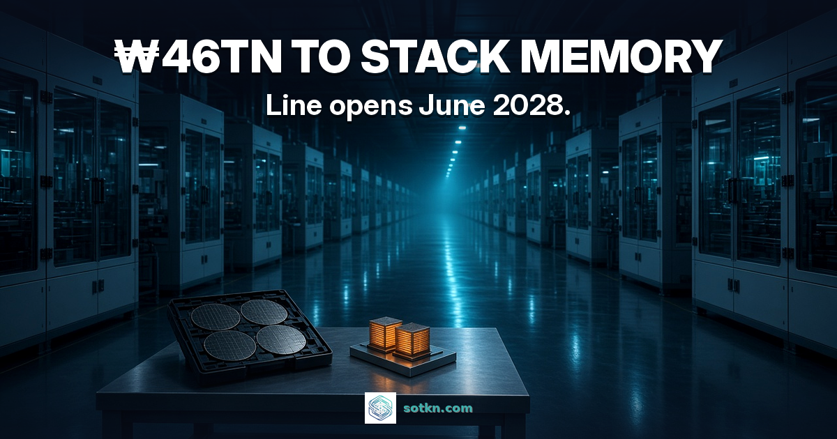
Samsung has sold all the HBM it can make next year, and its customers are asking for more. On 12 November it broke ground on the place where that memory gets finished: a ₩46 trillion plan to turn its old Onyang chip-testing campus into five lines that stack and test HBM. ₩40 trillion of it is equipment. The first new line opens in June 2028. The stuck step is the stacking line.
KOREA PULSE · SEMICONDUCTORS · HBM · ADVANCED PACKAGING · Data as at 14 Nov 2026 (Onyang groundbreaking 12 Nov; Samsung Q3 results 29 Oct; market close 13 Nov) · Next update: Korea’s November exports on 1 December
Affects: Semiconductors · Hyperscalers · AI Data Centers — Markets: Korea · Taiwan · US · China
Education only, not advice to buy or sell any security. ₩ is the Korean won; Samsung’s ₩46 trillion was reported as about US$34.5 billion, roughly ₩1,333 to the dollar. DRAM is the working memory in every server; HBM is many DRAM chips stacked on a small logic chip and placed right next to an AI chip (HBM explained). Our own sums are labelled. We wrote about Samsung’s third-quarter clean rooms on 30 October (Samsung’s Q3 clean rooms). That piece was about the front end, where memory wafers are made. This one is about the back end, where they are turned into HBM.
The numbers that matter this week
Onyang HBM plan
₩46tn
Five lines, phased · about US$34.5bn
NewOf which equipment
₩40tn
87% of the plan · buildings ₩6tn (our arithmetic)
Tools firstLine 5 clean room
31,000 m²
Three floors · campus 270,000 → 420,000 m²
BuildingStart date
June 2028
About a year earlier than planned
ClockSamsung chip capex, Q3
₩27.2tn
₩76.8tn planned for all of 2026
SpendingStacking and testing
2027 sold out
Shortage seen through 2028
Stuck stepYonhap and The Korea Times, 12 Nov 2026; Samsung Electronics Q3 2026 results, 29 Oct 2026. Status chips are Second Order’s read.
On this page: Why it matters · What was announced · What packaging does · Why the rush · The SK hynix race · Our math · Who gets paid · What is stuck? · Dates next · FAQ
Why does a packaging hall matter so much?
Think of a famous layer-cake shop. It bakes thin sponge layers in one kitchen across town. But nobody buys a pile of loose sponges. Each cake has to be stacked twelve or sixteen layers high, glued, trimmed and checked before it goes in the box. If the shop doubles its baking but keeps the same small stacking room, the extra sponges just sit on trays. The cakes customers have already paid for wait in a queue for the stacking table.
HBM works the same way. The memory chips are made on wafers in big fabs at Pyeongtaek and Hwaseong. The small logic chip at the bottom of each stack, the base die, is made in a foundry (the HBM base die). Neither is an HBM product yet. The chips have to be thinned, stacked, wired together through tiny vertical holes and tested as one block before Samsung can sell them to an AI chip maker. That finishing work is called packaging, or the back end, and it is what Onyang is being rebuilt to do.
So the question this groundbreaking answers is not “will Samsung make more memory?” It is “where will the extra memory be finished, and when?” The answer is: mostly at Onyang, with the first new line from June 2028. Until then, Samsung’s HBM output is limited by the stacking space and bonding tools it already has, however many wafers its fabs turn out.
What did Samsung announce on 12 November?
President Lee Jae Myung and Samsung Electronics chairman Lee Jae-yong broke ground together at the Onyang campus in Asan, South Chungcheong Province. The ceremony was the formal start of Samsung’s part of a government push to turn the central Chungcheong region into a hub for AI-era manufacturing. Onyang opened in 1991 as a place that assembled and tested ordinary chips. Lee Jae-yong said it would become a leading hub for HBM, which he called the heart of AI chips.
The plan has a few clear numbers. Samsung will invest ₩46 trillion in Onyang over the medium to long term to build five HBM production lines. Of that, ₩6 trillion is for construction and ₩40 trillion is for advanced equipment, which will go in step by step. Samsung stressed that the ₩46 trillion covers all five lines, not the cost of one building. The first piece is the campus’s fifth line: a three-storey building with about 31,000 square metres of clean room, where foundation work is now under way. It is due to start operating in June 2028, about a year ahead of the original schedule, according to Samsung’s chip chief Jun Young-hyun.
- Floor space: the campus grows from about 270,000 square metres to about 420,000 square metres once the plan is complete.
- Jobs: about 700 direct jobs at the new facility, and an average of 3,400 construction workers on site each day while it is built.
- Construction value: about ₩2.6 trillion of economic output from the building work, by Samsung’s estimate.
- Permits: South Chungcheong Province and Asan City cut the time for approvals to about a third of the usual period, so ground was broken about four months after Samsung announced the plan in July.
- Nearby: Samsung will also expand and modernise HBM facilities at its existing Cheonan site.
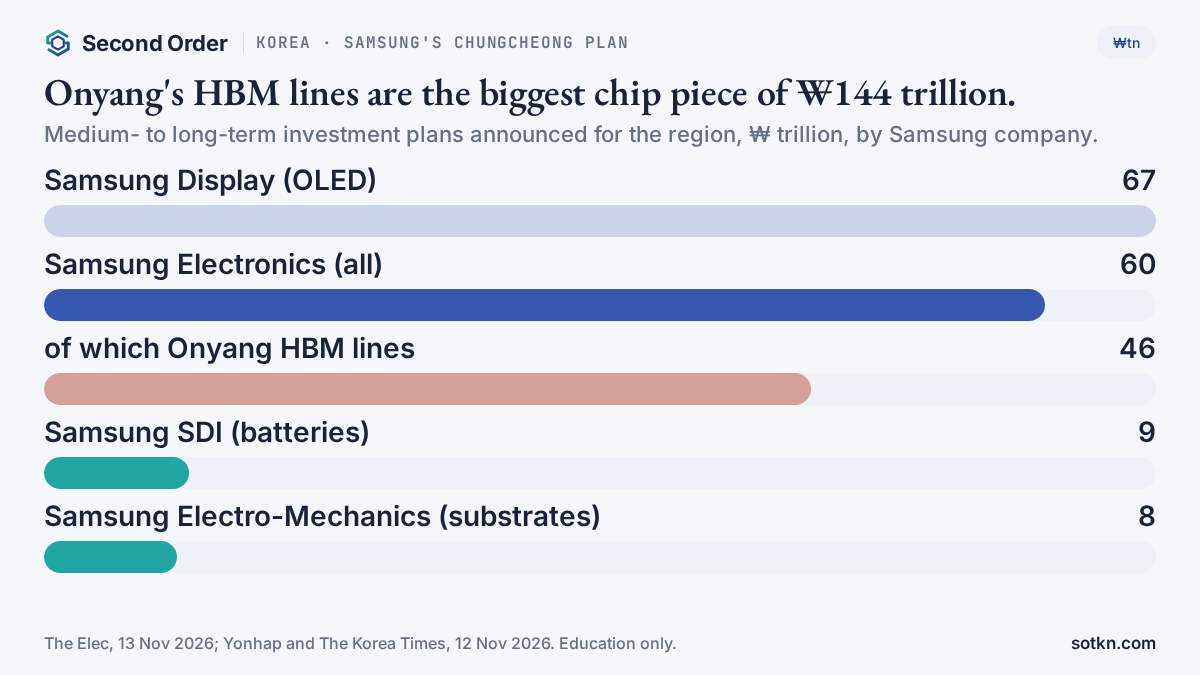
Onyang is one part of a wider group plan. Samsung and three affiliates put ₩144 trillion on the table for the region: ₩60 trillion from Samsung Electronics, ₩67 trillion from Samsung Display for new OLED screen lines, ₩8 trillion from Samsung Electro-Mechanics for AI server chip substrates, and ₩9 trillion from Samsung SDI for battery development. The same day marked the start of three projects at once: the Onyang packaging fab, a Samsung Display line in Asan and a Samsung Electro-Mechanics substrate plant in Sejong.
The government made a promise too. President Lee said central and local government would work as one team to handle all permits and put key infrastructure in place, naming power and water, so that investment plans in Chungcheong and in the south-west and south-east of the country go ahead without a hitch. A packaging line usually needs less power than a memory fab, but it still needs a substation, clean water and a steady supply of gases before tools can be switched on.
What does packaging actually do to HBM?
Samsung’s newest HBM, HBM4, shows the division of labour. The memory layers are its sixth-generation 10-nanometre-class DRAM, known as 1c DRAM, made in the memory fabs. The base die that controls the signals is made on a 4-nanometre logic process in Samsung’s foundry. Packaging brings them together: stacking the memory chips on the base die, connecting them, and testing the finished stack before it is shipped. Only then does it go to an AI chip maker, which places it beside its processor on a larger package (who makes advanced packaging).
The hard part is the bonding. Each memory chip is ground down to a fraction of the thickness of a hair, then pressed onto the one below with heat so that thousands of tiny connections line up. Samsung uses a method called TC-NCF, which puts a thin non-conductive film between the layers before they are pressed together. Its main rival, SK hynix, uses a different method in which the stack is built first and a liquid filler is injected afterwards. As the chips get thinner and the stacks taller, from 12 layers towards 16 and more, keeping them flat and lined up gets harder, and a bad bond can ruin a stack that already contains a dozen good chips.
That is why the machines matter. Samsung gets most of its HBM bonders from its own subsidiary, SEMES, and earlier this year Korean reports said it had chosen to stay with SEMES’s TC-NCF bonders for HBM4 rather than buy from Hanmi Semiconductor, an outside supplier. SK hynix, by contrast, switched to Hanmi’s bonders. So the ₩40 trillion of equipment is not one cheque to one company. It is bonders, testers and the many other tools a packaging line needs, bought line by line over several years (memory process tools for HBM).
Testing is the other half. A finished HBM stack is tested as one part, at speed, before it ships, because once it is placed beside an AI chip a fault is very expensive to fix. Better yield, meaning more good stacks out of each batch, is the same as more capacity. If a line raises its share of good stacks from six in ten to seven in ten, it gets about a sixth more sellable product from the same wafers (our arithmetic). Packaging space and yield together decide how many stacks a maker can sell.
Why is Samsung rushing the back end now?
Because the memory is already sold. At its third-quarter results on 29 October, Samsung reported revenue of ₩195.3 trillion and operating profit of ₩107.4 trillion, the first time any tech company had passed ₩100 trillion of quarterly operating profit. Its chip division alone made ₩106.5 trillion of operating profit on ₩147.1 trillion of revenue. The memory business set records for both, and Samsung said it had significantly scaled up sales of HBM4.
The outlook was tighter still. Samsung said AI-driven demand in 2027 will far exceed industry supply, more so than in 2026. It has finished negotiating its 2027 HBM volumes with customers, but they are asking for more, and it expects shortages to last through 2028. A seller in that position does not need to find buyers. It needs to make more finished product, and finished HBM comes out of a packaging line.
Samsung is spending to match. Its capital spending in the third quarter was ₩29 trillion, up ₩12.2 trillion from the second quarter, with ₩27.2 trillion of it in the chip division. For the whole of 2026 it expects about ₩84.4 trillion, ₩76.8 trillion of it in chips, for new fabs and other infrastructure. That implies about ₩24 trillion of chip spending still to come in the fourth quarter (our arithmetic).
The front end is moving on a matching clock. Samsung is adding 1c DRAM capacity for HBM4 at its fourth Pyeongtaek line, and has named 2028 as the year the fifth Pyeongtaek line starts as a key HBM production base. Onyang’s new line targets June of the same year. In other words, Samsung is trying to make sure that when the extra memory wafers arrive, there is somewhere to stack them. We looked at the front-end clean rooms in our Samsung company page and the October Pulse (what Samsung does).
How does this compare with SK hynix?
SK hynix, Samsung’s main HBM rival, is building its own back end on a similar clock. Its P&T7 plant in the Cheongju Technopolis industrial complex is a dedicated packaging and test plant for AI memory, including HBM. It broke ground in April 2026 on a 230,000-square-metre site, with about 150,000 square metres of clean room in total: a 60,000-square-metre wafer test line and a 90,000-square-metre wafer-level packaging line. The total plan is ₩19 trillion.
In July SK hynix’s board brought the first clean room forward by about three months, to as early as July 2027, and raised the first-phase construction budget to about ₩7.09 trillion without changing the ₩19 trillion total. The packaging line was planned to be finished in phases through February 2028. Here “finished” means the clean room is ready to receive tools, not that the line is making product. Contractors say the utility work for a clean room, from purchase orders to a clean, sealed room, usually takes 11 to 12 months.
SK hynix is also adding front-end fabs: in August it approved ₩54.3 trillion more for two of them, ₩35.2 trillion for its second Yongin fab, whose first clean room is scheduled for June 2029, and ₩19.1 trillion for M17 in Cheongju, targeting December 2028. We looked at how SK hynix’s own HBM back end is the step its share price leans on (SK hynix’s back-end stuck step) and at its third-quarter HBM4 numbers (SK hynix Q3).
The pattern is the same at both companies. Each is racing to have stacking space ready by 2027 and 2028, at about the time its new memory fabs come on. Neither is waiting for the fab first and the back end second. Both are building the two together, because a fab without a packaging line behind it makes wafers that cannot yet be sold as HBM.
What does the arithmetic say?
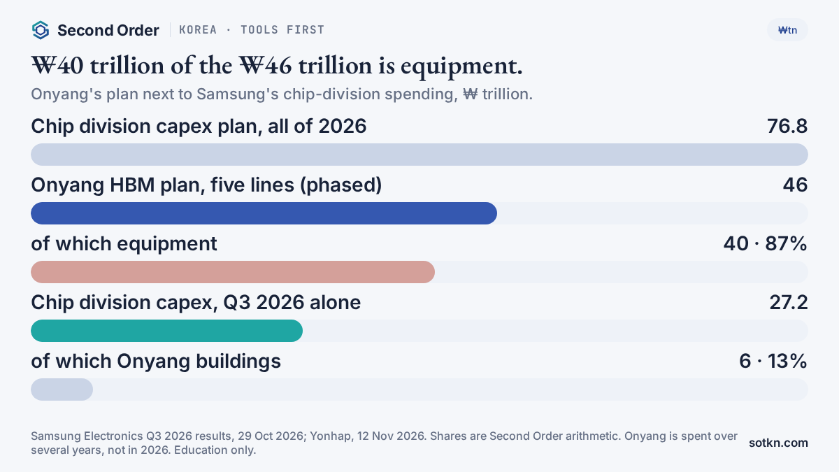
Everything below is our arithmetic from the published figures, not a Samsung forecast. Samsung has not said how the ₩46 trillion is split by year or by line, so the per-line figure is an average, not a budget.
- Tools share: ₩40 trillion of ₩46 trillion is about 87% equipment. Buildings are about 13%.
- Per line: ₩46 trillion over five lines averages about ₩9.2 trillion a line. Early lines may cost more or less.
- Against a year of spending: ₩46 trillion is about 60% of the ₩76.8 trillion Samsung plans to spend on chips in all of 2026, and about 1.7 times its chip spending in the third quarter alone. It is spread over several years.
- Against profit: ₩46 trillion is about 43% of the chip division’s ₩106.5 trillion operating profit in a single quarter. On today’s profits, Samsung can pay for the whole plan from less than half a quarter’s earnings.
- Floor space: 270,000 to 420,000 square metres is about 150,000 square metres more, an increase of about 56%.
- Line size: Onyang’s new line has about 31,000 square metres of clean room, about a fifth of the roughly 150,000 square metres planned at SK hynix’s P&T7. The two are not like for like: P&T7 includes a large wafer test line, and Onyang has four more lines to come.
- Clock: from the groundbreaking on 12 November 2026 to June 2028 is about 19 months. For comparison, P&T7 needed about 15 months from groundbreaking to its first clean room.
- Suppliers: 194 Korean materials, parts and equipment companies plan about ₩18.1 trillion of investment by 2030, about ₩93 billion each on average. The 66 investing in Chungcheong plan ₩4.4 trillion.
The arithmetic says two things. The money is not the constraint: Samsung can fund this out of current profit many times over. And most of the money is tools, which have to be ordered, built, delivered, installed and tuned before the line makes a single stack. That is where the wait sits.
Onyang and the race for HBM back ends
Yonhap, The Korea Times and Aju Press, 12 Nov 2026; The Elec, 23 Jul and 13 Nov 2026; Samsung Electronics, 29 Oct 2026. Sums marked as ours are Second Order arithmetic.
Who gets paid, and who waits?
1 · Equipment makers
Who: Bonding, stacking and test tools; SEMES supplies Samsung’s bonders
Paid: ₩40tn, paid as tools are delivered
2 · Builders and utility contractors
Who: Three-storey hall, clean room, power, water, gases
Paid: ₩6tn, paid while the hall goes up
3 · Substrates and suppliers
Who: Samsung Electro-Mechanics Sejong; 194 suppliers ₩18.1tn
Paid: Paid as their own plants fill
4 · Samsung
Who: Sells finished HBM stacks to AI chip makers
Paid: Paid when stacks ship, from June 2028 for this line
5 · Stacking and testing
Who: 2027 sold out; shortage through 2028
Paid: Sets how many stacks can be sold
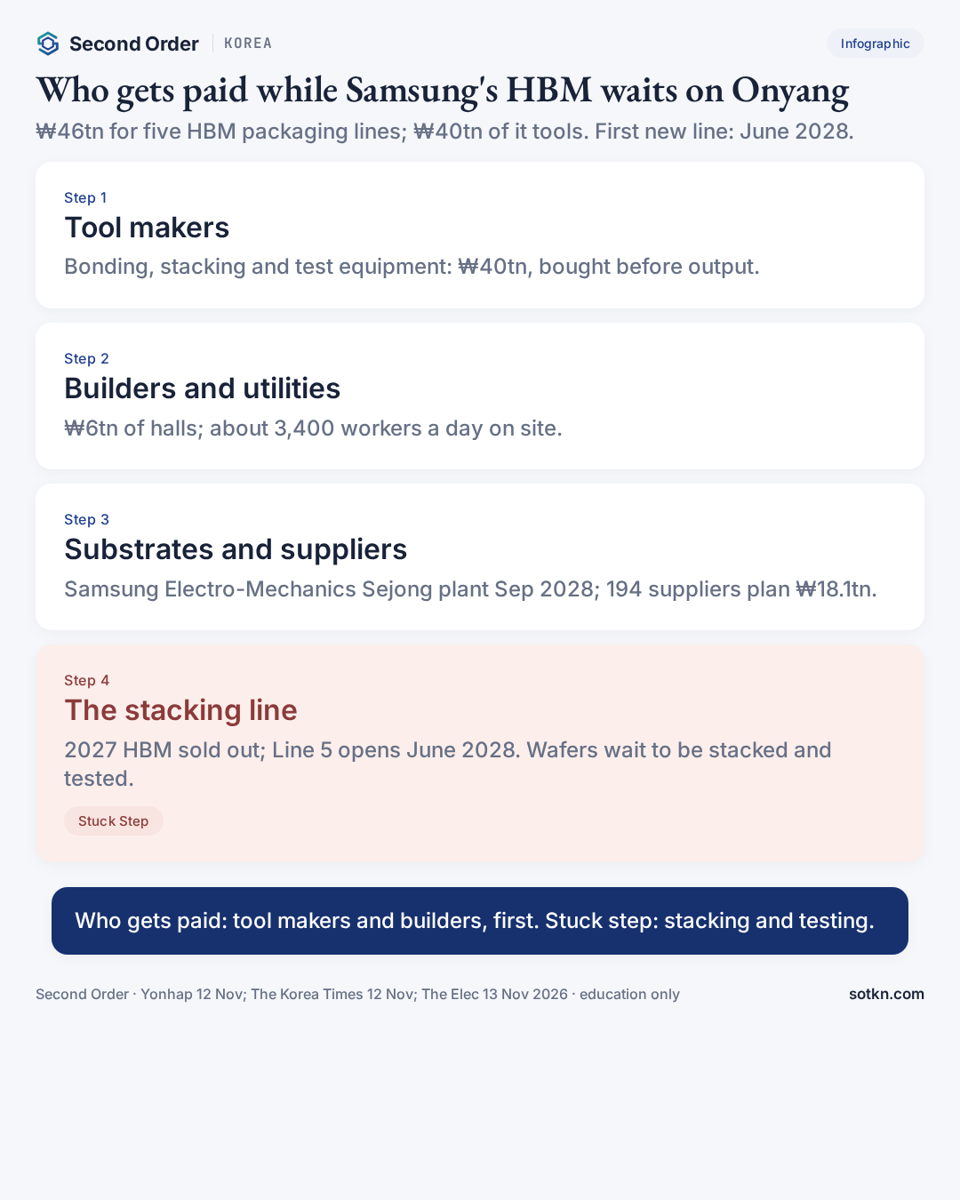
First in line are the equipment makers. Tools are 87% of the plan, and they are paid for when they are delivered and accepted, long before the line sells anything. For Samsung’s bonders, the biggest single beneficiary is likely to be SEMES, Samsung’s own equipment subsidiary, which keeps that money inside the group. Testers, inspection tools, wafer grinders and the many machines around them come from a wider list of Korean and foreign suppliers. Samsung has not named the vendors for Onyang, and we do not guess.
Second, the builders and utility contractors. The ₩6 trillion for construction pays for the halls, the clean rooms and the systems under them: power distribution, ultra-pure water, exhaust, chemicals and gas lines. Samsung puts the construction work at about ₩2.6 trillion of economic output, with 3,400 people on site on an average day. These firms are paid as the building rises, so their money arrives in 2027 and early 2028, well before the line runs.
Third, the substrate makers and other suppliers, who are paid later and in smaller pieces. Samsung Electro-Mechanics is spending about ₩4.27 trillion on a new plant in Sejong for the flip-chip substrates that sit under AI server chips, with mass production from September 2028 (who makes IC substrates). The head of Samsung’s supplier council, Daeduck Electronics chairman Kim Young-jae, said 194 domestic suppliers plan to invest about ₩18.1 trillion by 2030. Their sales grow only as Samsung’s lines fill.
Fourth, Samsung itself, which pays everyone above and is paid last for this line. Its HBM sells today from existing capacity, and its 2027 volumes are already agreed. The extra stacks from Onyang’s new line can only be sold once the line is built, tooled, qualified and running, from June 2028 at the earliest. Until then the ₩46 trillion is cost, not revenue.
Who waits: the AI chip makers and, behind them, the cloud companies. They have already been told 2027 is sold out. More Korean HBM in 2028 depends partly on lines like this one opening on time (the Hyperscalers layer).
What is stuck, exactly?
The stuck step is the finishing step for HBM: stacking and testing. Samsung is not short of money, and on its own account it is not short of buyers. It is short of finished HBM, and the amount of finished HBM it can sell is limited by how many stacks its packaging lines can bond and test each month. A new memory wafer that cannot be stacked is not yet revenue.
The clock has three parts. First the building: foundation work is under way now, and the three-storey hall and its clean room must be finished, sealed and cleaned. Second the tools: ₩40 trillion of equipment has to be built by suppliers who are serving every memory maker at once, delivered and installed. Third the qualification: a new line has to show its stacks meet a customer’s standards before they can ship in volume. June 2028 is when the line is due to start, which is not the same as full output.
There are honest reasons for caution. An industry source told Aju Press the year-early schedule was hard to verify independently. Fabs and packaging lines in Korea also depend on power and water arriving on time, which is why the president named both; we have written before about how fast-tracked chip sites still wait on power lines (fast-track vs power lines). And demand is not guaranteed. Nvidia said on 12 November, US time, that its chief executive Jensen Huang had stepped down, with finance chief Colette Kress named interim chief executive. No change to Nvidia’s HBM buying has been announced, and on 13 November Korea’s science minister said Nvidia had confirmed its plan to deploy up to 260,000 GPUs in Korea with Korean partners.
The market took the news calmly on the day and nervously the day after. On 13 November the KOSPI fell 0.98% to 5,290.53 as foreign investors sold. Samsung Electronics closed down 0.48% at ₩207,000, SK hynix down 2.47% at ₩1,223,000 and Samsung Electro-Mechanics down 2.93% at ₩860,000. One day’s prices say more about Nvidia’s news than about Onyang, and we draw no conclusion from them.
It is not the money, which Samsung can fund many times over. It is not, for now, demand, since 2027 is sold out. It is the stacking line, and how fast a building, its tools and its first good stacks can be made ready. It is the same shape we keep finding: the slow step sets the timing for everyone else, and the money gathers at the scarce step (where the stuck step moves). Our explainer on the memory makers found the binding limit was clean-room space for new memory lines (who makes DRAM). For HBM, Onyang shows the same limit one step later: clean-room space for stacking.
Which dates test the read?
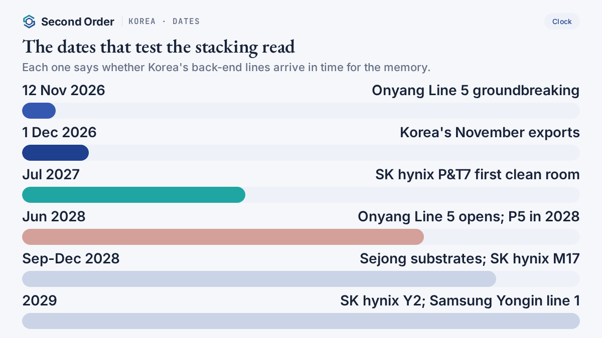
- 12 November 2026 — Onyang Line 5 groundbreaking; ₩46 trillion plan for five HBM lines.
- About 21 November 2026 — Korea Customs’ count for 1–20 November: are chip exports still rising this fast?
- 1 December 2026 — Korea’s full November exports.
- Late January 2027 — Samsung’s board meets to set its next shareholder return policy and the rest of its 2026 payout.
- July 2027 — SK hynix’s P&T7 packaging plant opens its first clean room, if the faster schedule holds.
- 2028 — Samsung’s fifth Pyeongtaek line starts as an HBM production base.
- June 2028 — Onyang Line 5 starts operating.
- September 2028 — Samsung Electro-Mechanics’ Sejong substrate plant begins mass production.
- December 2028 and June 2029 — SK hynix’s M17 and the first clean room of its second Yongin fab.
Dates from Yonhap and The Korea Times (12 Nov 2026), The Elec (23 Jul and 13 Nov 2026), Aju Press (13 Nov 2026) and Samsung Electronics (29 Oct 2026). The 21 November customs date is the usual timing, not an announced one.
How does this look from Taiwan, the US and China?
From Taiwan, Korean HBM is the input that sets the pace. This morning’s Taiwan Pulse found Korea had become Taiwan’s biggest single supplier for the first time, on memory (Korea is now Taiwan’s biggest supplier). Taiwan’s chip packagers then put that HBM beside AI chips on a larger package, a step with its own queue (advanced packaging on the Wire). From the US, the buyers are the AI chip designers and cloud companies who have been told 2027 is sold out (US Markets). From China, the comparison is with domestic memory makers trying to build their own HBM with far fewer tools (China Markets). Korea sits at the start of that chain: it makes the memory, and now it is building the place to finish it.
How we check this. The Onyang figures come from Samsung’s own statements at the 12 November groundbreaking as reported by Yonhap, The Korea Times, The Elec and Aju Press: the ₩46 trillion plan, its split, the clean-room size, the June 2028 start and the floor space. Samsung’s spending, profit and outlook come from its third-quarter results release of 29 October. SK hynix’s packaging schedule comes from its board disclosures as reported by The Elec. Market prices are 13 November closing levels. Every sum we worked out is labelled “our arithmetic”. Samsung has not said how much HBM the new line will make, so we do not guess a stack count or a revenue figure. An industry source told Aju Press the year-early schedule was hard to verify independently, and we flag that where it matters. Price targets and ratings are left out on purpose. The references we used are listed at the end. Our editorial standards →
FAQ
What did Samsung announce at Onyang?
On 12 November 2026 Samsung Electronics broke ground on a fifth production line at its Onyang campus in Asan, South Chungcheong Province. Over time it plans to spend ₩46 trillion, about US$34.5 billion, on five lines for packaging HBM, the stacked memory used beside AI chips: ₩6 trillion for buildings and ₩40 trillion for equipment, in phases. The first new line, with a 31,000-square-metre clean room, is due to start in June 2028, about a year earlier than first planned.
What does HBM packaging mean?
HBM is made of many thin DRAM chips stacked on top of a small logic chip called a base die. The chips are made in separate factories. Packaging is the step that thins them, stacks them, connects them through tiny vertical wires and tests the finished stack before it is sold to an AI chip maker. Without that step, a finished memory wafer is not yet an HBM product.
Who gets paid first?
The equipment makers and builders. Of the ₩46 trillion, ₩40 trillion is for tools, and tools are bought and paid for before the line makes anything. Builders and utility contractors are paid while the hall goes up. Samsung itself is paid only when finished HBM ships, from June 2028 on for this line.
What is the stuck step?
The finishing step for HBM: stacking and testing. Samsung says its 2027 HBM is sold out and shortages last through 2028. More memory wafers only become more HBM if there is packaging space and bonding tools to stack them, and the first new Onyang line is about 19 months away.
Is this investment advice?
No. Education only. It maps who gets paid and which step is stuck. It is not a recommendation to buy or sell any security, and we leave out price targets and ratings on purpose.
References
Outbound links below are nofollow. We list only the sources actually used. Internal sotkn.com links in the body are separate.
- Yonhap News Agency, Samsung Electronics chief vows to turn Onyang campus into HBM hub, 12 Nov 2026. en.yna.co.kr — the ₩46 trillion plan for five HBM lines, the ₩6 trillion and ₩40 trillion split, the 31,000-square-metre clean room, the June 2028 start, the floor-space expansion and the 700 jobs.
- The Korea Times, Samsung Electronics breaks ground on new HBM packaging facility in Asan, 12 Nov 2026. koreatimes.co.kr — the year-early schedule, the 3,400 daily construction workers and ₩2.6 trillion of construction output, permits cut to a third, and Samsung’s comments that 2027 HBM volumes are agreed and shortages last through 2028.
- The Elec, Samsung Begins 144 Trillion Won Investment in South Korea’s Chungcheong Region, 13 Nov 2026. thelec.net — the ₩144 trillion split across Samsung Electronics, Samsung Display, Samsung Electro-Mechanics and Samsung SDI, Cheonan, the substrate plant in Sejong, and the 194 suppliers planning ₩18.1 trillion by 2030.
- Aju Press, Samsung breaks ground on $34 billion HBM packaging hub in Asan, 12 Nov 2026. ajupress.com — Jun Young-hyun’s June 2028 target and an industry source’s caution that the reported acceleration is hard to verify independently.
- Aju Press, AI bust? Korea presses on with chip republic despite Huang setback, 13 Nov 2026. ajupress.com — how HBM4 joins 1c DRAM with a 4-nanometre base die, why more DRAM becomes more HBM only if packaging keeps up, Pyeongtaek P5 in 2028 and SK hynix’s Y2 and M17 schedules.
- Samsung Electronics, Third Quarter 2026 Results, 29 Oct 2026. news.samsung.com — Device Solutions revenue and operating profit, third-quarter and full-year capital spending, and the outlook that AI demand will far exceed supply in 2027.
- The Elec, SK Hynix to Open Cheongju P&T7 Cleanroom Three Months Ahead of Schedule, 23 Jul 2026. thelec.net — SK hynix’s ₩19 trillion P&T7 packaging and test plant, its July 2027 first clean room, its line sizes and the 11 to 12 months a clean room takes to be ready.
- Alpha Biz, Samsung Semiconductor Will Not Use Hanmi TC Bonder Equipment, 24 Feb 2026. alphabiz.co.kr — Samsung staying with TC-NCF bonders from its own subsidiary SEMES for HBM4, and why the bonding method matters as stacks get taller.
- Yonhap News Agency, Nvidia confirms planned supply of GPUs to S. Korea despite Jensen Huang’s resignation, 13 Nov 2026. en.yna.co.kr — the science minister’s statement that Nvidia still plans up to 260,000 GPUs in Korea.
- Aju Press, Korean stocks reverse early gains as foreigners shift to selling, 13 Nov 2026. ajupress.com — the 13 November closing levels for the KOSPI, Samsung Electronics, SK hynix and Samsung Electro-Mechanics.
Not investment advice. Do your own research. Education only. Map of who gets paid and which step is stuck — not a buy list.
More on this desk: Korea Markets · Semiconductors · who makes HBM · clean rooms explained · Korea’s October exports · all Markets.